

FantomXR
-
Posts
1,035 -
Joined
-
Last visited
-
Days Won
22
Content Type
Profiles
Forums
Blogs
Gallery
Posts posted by FantomXR
-
-
Hey people,
I'd like to add one or two chip-selects for the AINSER8. I've already made a few changes to the firmware but it's not working yet.
Under modules I've edited the ainser.c:
{ switch( module ) { case 0: return MIOS32_SPI_RC_PinSet(AINSER_SPI, AINSER_SPI_RC_PIN_MODULE1, value); // spi, rc_pin, pin_value case 1: return MIOS32_SPI_RC_PinSet(AINSER_SPI, AINSER_SPI_RC_PIN_MODULE2, value); // spi, rc_pin, pin_value case 2: return MIOS32_SPI_RC_PinSet(AINSER_SPI, AINSER_SPI_RC_PIN_MODULE3, value); // spi, rc_pin, pin_value #if AINSER_NUM_MODULES > 3 # error "CS Line for more than 2 modules not prepared yet - please enhance here!" #endif }and ainser.h:
// Which RC pin of the SPI port should be used for the third module // allowed values: 0 or 1 for SPI0 (J16:RC1, J16:RC2), 0 for SPI1 (J8/9:RC), 0 or 1 for SPI2 (J19:RC1, J19:RC2) #ifndef AINSER_SPI_RC_PIN_MODULE3 #define AINSER_SPI_RC_PIN_MODULE3 2 #endifand mios32_spi,h
#define MIOS32_SPI2_RCLK1_PORT GPIOA // RC1 #define MIOS32_SPI2_RCLK1_PIN GPIO_Pin_15 #define MIOS32_SPI2_RCLK1_AF { GPIO_PinAFConfig(GPIOA, GPIO_PinSource15, GPIO_AF_SPI3); } // only relevant for slave mode #define MIOS32_SPI2_RCLK2_PORT GPIOB // RC2 #define MIOS32_SPI2_RCLK2_PIN GPIO_Pin_8 #define MIOS32_SPI2_RCLK2_AF { } #define MIOS32_SPI2_RCLK3_PORT GPIOC // RC3 #define MIOS32_SPI2_RCLK3_PIN GPIO_Pin_1 #define MIOS32_SPI2_RCLK3_AF { }#else MIOS32_SPI2_RCLK1_AF; MIOS32_SPI2_RCLK2_AF; MIOS32_SPI2_RCLK3_AF; MIOS32_SPI2_SCLK_AF; MIOS32_SPI2_MISO_AF; MIOS32_SPI2_MOSI_AF; if( slave ) { // SCLK and DOUT are inputs assigned to alternate functions GPIO_InitStructure.GPIO_Mode = GPIO_Mode_AF; GPIO_InitStructure.GPIO_Pin = MIOS32_SPI2_SCLK_PIN; GPIO_Init(MIOS32_SPI2_SCLK_PORT, &GPIO_InitStructure); GPIO_InitStructure.GPIO_Pin = MIOS32_SPI2_MOSI_PIN; GPIO_Init(MIOS32_SPI2_MOSI_PORT, &GPIO_InitStructure); // RCLK (resp. CS) are configured as inputs as well GPIO_InitStructure.GPIO_Mode = GPIO_Mode_AF; GPIO_InitStructure.GPIO_Pin = MIOS32_SPI2_RCLK1_PIN; GPIO_Init(MIOS32_SPI2_RCLK1_PORT, &GPIO_InitStructure); GPIO_InitStructure.GPIO_Pin = MIOS32_SPI2_RCLK2_PIN; GPIO_Init(MIOS32_SPI2_RCLK2_PORT, &GPIO_InitStructure); GPIO_InitStructure.GPIO_Pin = MIOS32_SPI2_RCLK3_PIN; GPIO_Init(MIOS32_SPI2_RCLK3_PORT, &GPIO_InitStructure); // DOUT is output assigned to alternate function GPIO_InitStructure.GPIO_Mode = GPIO_Mode_AF; GPIO_InitStructure.GPIO_Pin = MIOS32_SPI2_MISO_PIN; GPIO_Init(MIOS32_SPI2_MISO_PORT, &GPIO_InitStructure); } else { // SCLK and DIN are inputs GPIO_InitStructure.GPIO_Mode = GPIO_Mode_AF; GPIO_InitStructure.GPIO_Pin = MIOS32_SPI2_SCLK_PIN; GPIO_Init(MIOS32_SPI2_SCLK_PORT, &GPIO_InitStructure); GPIO_InitStructure.GPIO_Pin = MIOS32_SPI2_MOSI_PIN; GPIO_Init(MIOS32_SPI2_MOSI_PORT, &GPIO_InitStructure); // RCLK (resp. CS) are configured as inputs as well GPIO_InitStructure.GPIO_Mode = GPIO_Mode_OUT; GPIO_InitStructure.GPIO_Pin = MIOS32_SPI2_RCLK1_PIN; GPIO_Init(MIOS32_SPI2_RCLK1_PORT, &GPIO_InitStructure); GPIO_InitStructure.GPIO_Pin = MIOS32_SPI2_RCLK2_PIN; GPIO_Init(MIOS32_SPI2_RCLK2_PORT, &GPIO_InitStructure); GPIO_InitStructure.GPIO_Pin = MIOS32_SPI2_RCLK3_PIN; GPIO_Init(MIOS32_SPI2_RCLK3_PORT, &GPIO_InitStructure); // DIN is input with pull-up GPIO_InitStructure.GPIO_Mode = GPIO_Mode_AF; GPIO_InitStructure.GPIO_PuPd = GPIO_PuPd_UP; GPIO_InitStructure.GPIO_Pin = MIOS32_SPI2_MISO_PIN; GPIO_Init(MIOS32_SPI2_MISO_PORT, &GPIO_InitStructure); }#else switch( rc_pin ) { case 0: MIOS32_SYS_STM_PINSET(MIOS32_SPI2_RCLK1_PORT, MIOS32_SPI2_RCLK1_PIN, pin_value); break; case 1: MIOS32_SYS_STM_PINSET(MIOS32_SPI2_RCLK2_PORT, MIOS32_SPI2_RCLK2_PIN, pin_value); break; case 2: MIOS32_SYS_STM_PINSET(MIOS32_SPI2_RCLK3_PORT, MIOS32_SPI2_RCLK3_PIN, pin_value); break; default: return -4; // unsupported RC pin } break; #endifIn the NGC I have:
AINSER n=1 enabled=1 cs=2 num_pins=1and nothing happens. Which part do I overlook for adding a CS?
Thanks!
Chris -
The plan is not to use encoders. I'd like to use sin/con potentiometers, which will be connected to a MSP430 uC (which converts these signals to encoder-typical signals). So the whole circuit needs only 3V3. I'd like to avoid routing two supply rails on my PCB.
-
1 hour ago, Antichambre said:
But you can use HCT595/165 and remove the 541 on your own design. Keep in mind HCT need 5V supply voltage.
Yes. But I could use LV165 or not? That could be supplied with 3V3.
-
I have another question regarding the ICs.
For what reason do we use the HCT541? It does level-shifting and buffering. So if we want to drive only small distances, this might be obsolete? And if we take HCT595 and HCT165 the level of the signals the STM outputs should fit or not?
-
You can chain them via midi I/O easily.
If you want to connect multiple midiboxes via USB you would need to define different USB descriptions in the firmware which means you need to be able to compile firmwares by yourself.
-
If I understood him correctly he wants to avoid the Arduino solution. It will make things a lot more complicated. But an Arduino can drive tons of LEDs without problems. That's why he uses it.
Let's see what he says :-)
-
3 hours ago, TK. said:
It shouldn't be a big deal to optimize the memory consumption. There are various places in MIOS32 where I already used DMA double buffers (e.g. I2S audio output). Nothing needs to be explored, just translation :)
That sounds great! And... are you willing to do so? :-D
Awesome work @Antichambre. Looks fabulous. Could you tell us where you have the translucent PMMA from? I buy my materials at TroTec. They have also awesome stuff!
-
Thanks for your explanation, pictures and videos.
Well, as I told you in an email already you really should think about, going down with the LED-count while keeping the diameter as is now. This will give you some space between the LEDs and it should be very easy creating a mask for it so you don't have any crossbleeding ;-)
-
I don't want them to be detented.
-
Hey people,
I'm looking for encoders. The pinout doesn't matter as well as the gird. The only thing that is important is, that they have a great feel. All encoders I've tested (PEC11, PEC12, PEC16, EC12, EC16) are too "light" so to say. There is no resistance when turning the knob. I need encoders that need more torque to get turned.
Any ideas where I can find those?
Best,
Chris -
Looks great! :-)
-
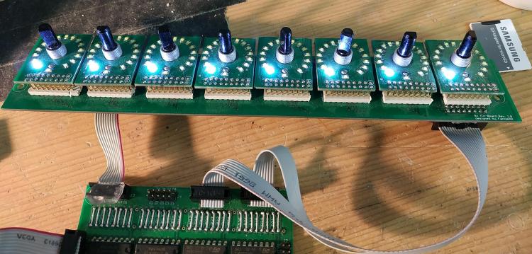
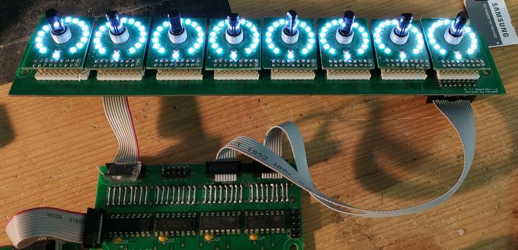
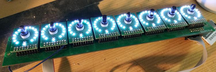
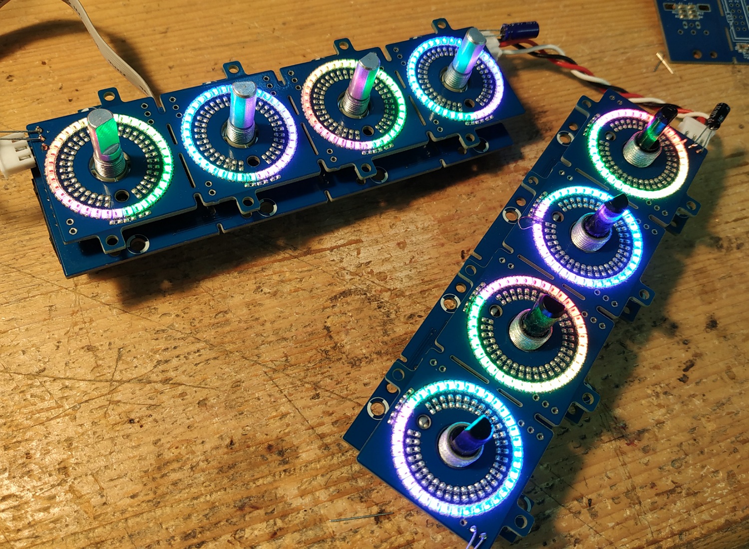
Hey people,
thanks to @TK.! It's working great.
Anyway I had still some flickering on the LEDs. As I stated above I left away the caps ... and this was the reason. I know have added a 10uF on the input and on the output-connector of the LED-rings and the flickering is completely eliminated! Great!!
So, one core can handle a total of 10 LED (10*36=360) rings....

-
 1
1
-
-
Hey Thorsten,
Great! I'll test it tomorrow with the rings.
So, what do you think is the limit regarding led-count?
Thank you very much!
Chris
-
I can confirm that 2.42" is working great too!

-
Hey people,
we could need some help on this project.
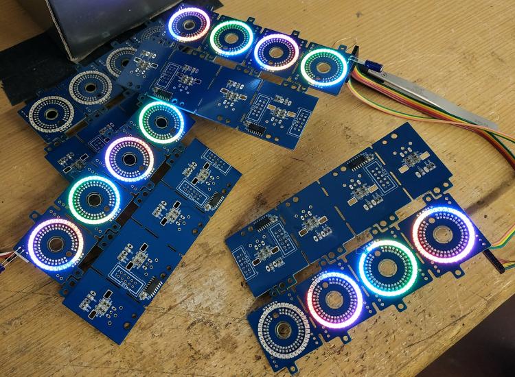
So far the pick and place machine did a great job and the reflow oven as well. So I now have a few boards to test.
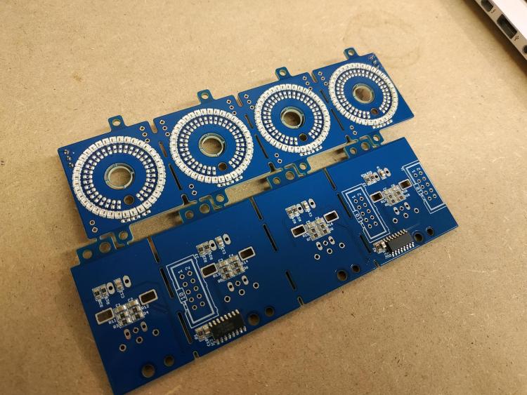
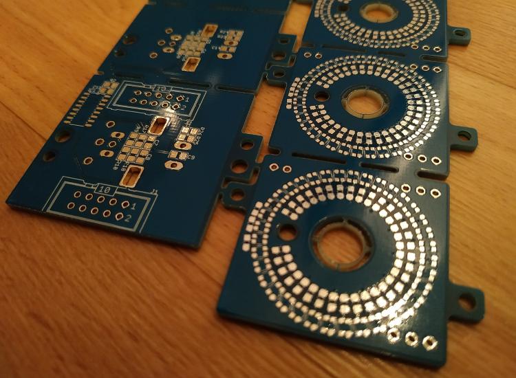
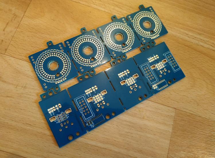
But I already run into a problem. In the firmware I set WS2812_NUM_LEDS to 144, because one prototype board is made from 4x36 LEDs => 144. Compiled and flashed. The core boots up nicely.
As stated in my previous post, the last 5 or 6 LEDs are slightly flickering. I've tested inserting 5V at the end of the LEDs again but this doesn't change anything. So it doesn't seem to be a power-related problem.Things start to get crazy if I connect another LED-ring-board in series with the first. I set WS2812_NUM_LEDS to 180 (with 190 the core doesn't boot anymore), compiled and flashed. I think a video can describe better what happens here:
https://www.dropbox.com/s/b5phnsji4k9wjhs/YI051501.mp4?dl=0
Does anyone know where this could come from?! Also does someone has an idea why the cores do not boot anymore as soon as I set WS2812_NUM_LEDS to 190 and more?
Any help would be very appreciated.
Thanks,
Chris -
So, I made some progress today.
I've tested it on another core (which I designed myself) and there the LEDs were running with the stock-firmware. No changes were needed. So I pick&placed 3 1/3 boards today.
What I still don't get why it doesn't work on a core with a discovery-board. Both ran the same firmware...
But I ran into another problem. In my first test I set WS2812_NUM_LEDS to 140. I compiled the firmware and flashed it. It was running fine except that LED 139 and 140 were flickering. Not sure if this is a sign of RAM-overload or if it was power-related. well... I don't think it's power-related though because they were also flickering if only they were turned on and all other LEDs off.
Next I tried to set WS2812_NUM_LEDS to 300. I compiled and flashed the firmware. Result: The core doesn't boot anymore. Since my own core doesn't have a user-button I have to reflash the bootloader through SWD. I don't have time the next days to try it. But I wanted to give you an update on this.
And here is a short video of my p&p-machine... it wass running slow because it was a first test.https://www.dropbox.com/s/89zfhdda1sc2f45/VID_20190510_151248.mp4?dl=0
By the way: I left out the filter-caps because I normally don't work with 0603 parts and though don't have them in my workshop and don't have them in my machine. Should be okay for the prototypes.
-
1
-
-
On 8.5.2019 at 3:25 PM, weasel said:
it is 105 CPU cycles which at 168 MHz amount to 1.25uS.
This calculation is not clear to me.
1 CPU cycle @ 168MHz is about 0,006uS
105 x 0,006 = 0,63uSOr not?
-
Help needed! :-(
I try to adapt the code to work with the WS2812-2020. I have to edit the ws2812.c because the 2020-version runs at 2kHz instead at 800kHz.
So I try to understand what happens here. This is the original code:// timers clocked at CPU/2 clock, WS2812 protocol requires 800 kHz (1.25 uS period) #define WS2812_TIM_PERIOD ((MIOS32_SYS_CPU_FREQUENCY/2) / 800000) #define WS2812_TIM_CC_RESET 0 #define WS2812_TIM_CC_IDLE WS2812_TIM_PERIOD #define WS2812_TIM_CC_LOW (u16)((WS2812_TIM_PERIOD - 1) * 0.28) // 28% -> ca. 0.35 uS #define WS2812_TIM_CC_HIGH (u16)((WS2812_TIM_PERIOD - 1) * 0.74) // 74% -> ca. 0.90 uS // DMA channel (DMA1 Stream 0, Channel 2 - fortunately DMA1_Stream0 not used by any other MIOS32 driver yet...!) #define WS2812_DMA_PTR DMA1_Stream0 #define WS2812_DMA_CHN DMA_Channel_2 #define WS2812_BUFFER_SIZE ((WS2812_NUM_LEDS+10)*24) // +10*24 to insert the RESET frame of 10*24*1.25 = 300 uSMIOS32_SYS_CPU_FREQUENCY should be 168000000, found in mios32_sys.h. But if I type this into a calculator:
(168000000 / 2) / 800000 = 105
So, why is 105 == 1.25uS? Doesn't make any sense to me....Any help?
Here is the datasheet of the 2020:
https://www.tme.eu/Document/4a8239e52df5e0b5cc2eb96834c5d8b6/WS2812B-2020.pdfAnd here of the 4040:
https://cdn-shop.adafruit.com/datasheets/WS2812B.pdf -
Dear Bruno,
not sure, what do you mean. Could you explain please?
Best,
Chris -
Yes... they look pretty :-)
-
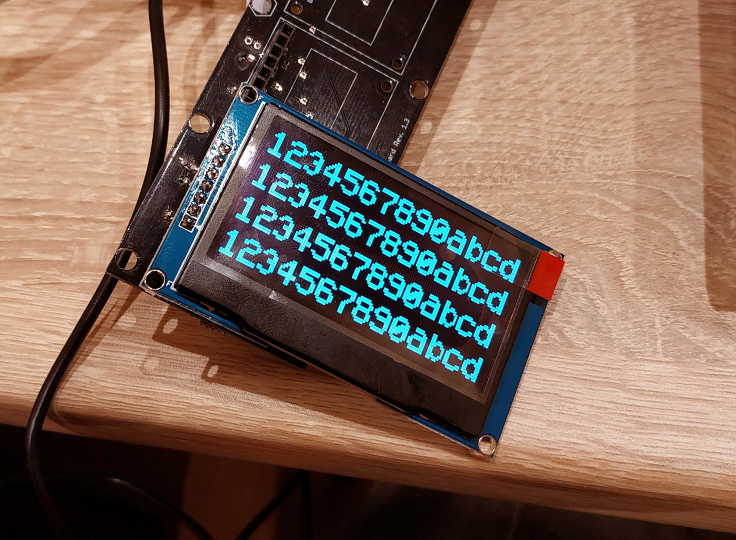
Here a picture... see the standard 0.96" in the background how small it is...
-
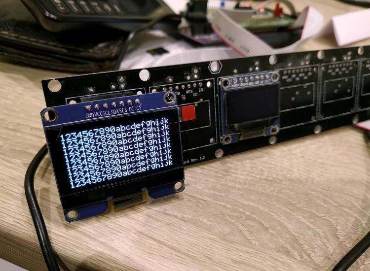
Hey people,
I just want to inform you, that I've got a SSD1309 display here and it works perfectly well with NG without any changes on the firmware! :-)
The screen next to me is 1.54". There is also a 2.42" version, which I also ordered but it has not arrived yet. This one has also SSD1309 :-D
Awesome displays!
Best,
Chris -
By the way: all prices are "or best offer". Id like to get rid of those parts. So if you are interested just drop me a PM.
-
Hey people,
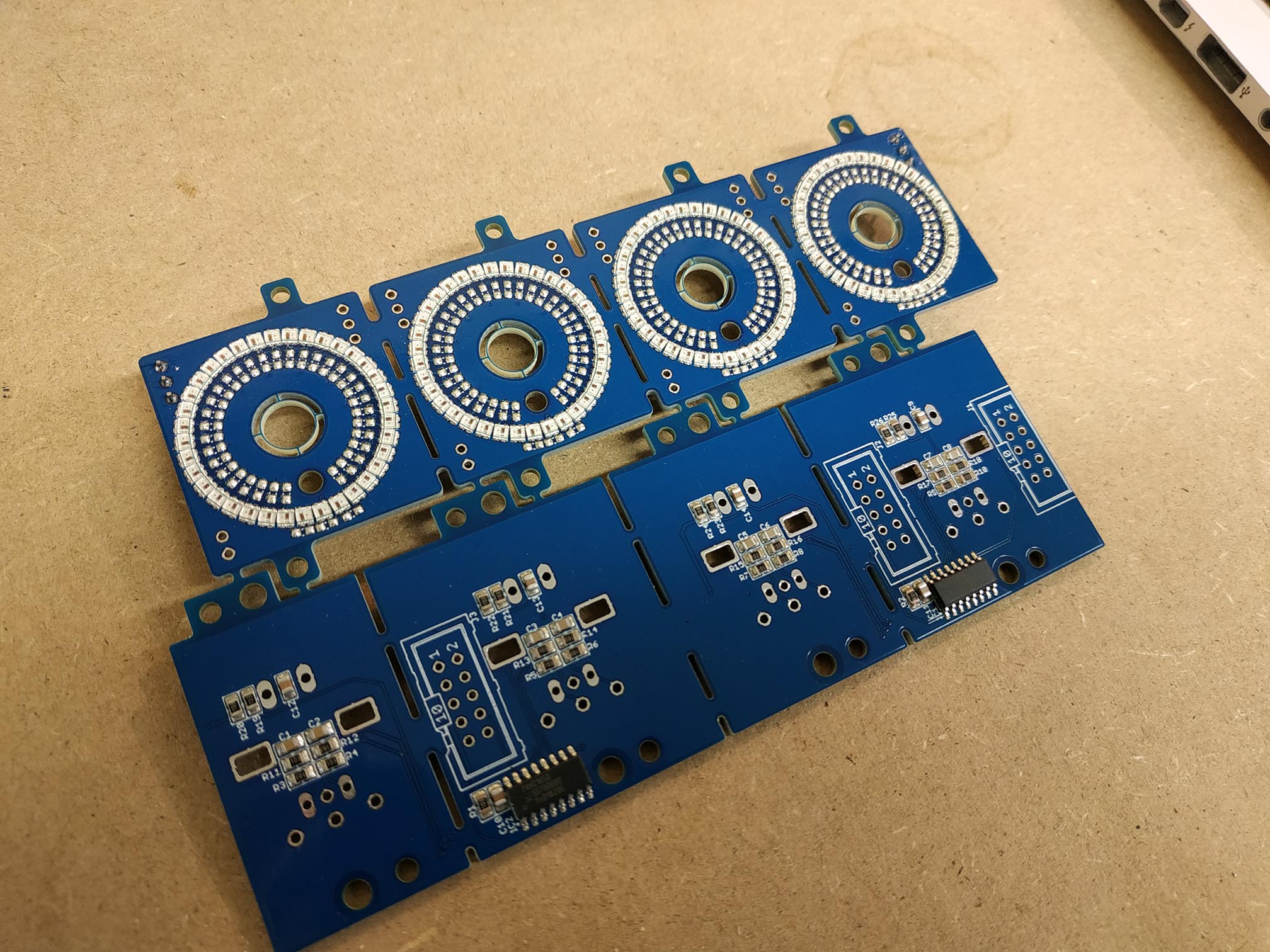
I cleaned up my room a bit and found some PCBs I do not need anymore. Here we go:
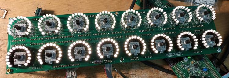
This is something I developed years ago! It has a PCB with 8 encoders with LED rings. Although they look blue, they are not. The LEDs (0603) are white! As you can see the PCB an be connected to a standard DOUT-module even without any resistors. The LEDs won't get damaged. I did a mistake in the wiring of the LEDs at this point. So if you follow the official LED-Matrix-Pattern, you will get crazy results. But anyway: This is a software-thing. If you change the matrix-pattern, they work perfectly. I'll advice you about it if you buy it.
I have two of those available. On one of them I needed to fix a trace (3rd. picture on the left). But it's perfectly working.
Encoders are Bourns PEC16 with integrated switch. Underneath there are three IDC connectors for the encoders and switches that can be directly connected to a DIN-module.
Price: 30€ each o.b.o.
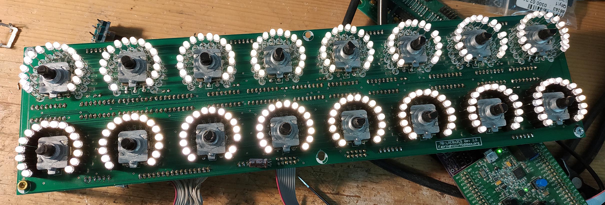
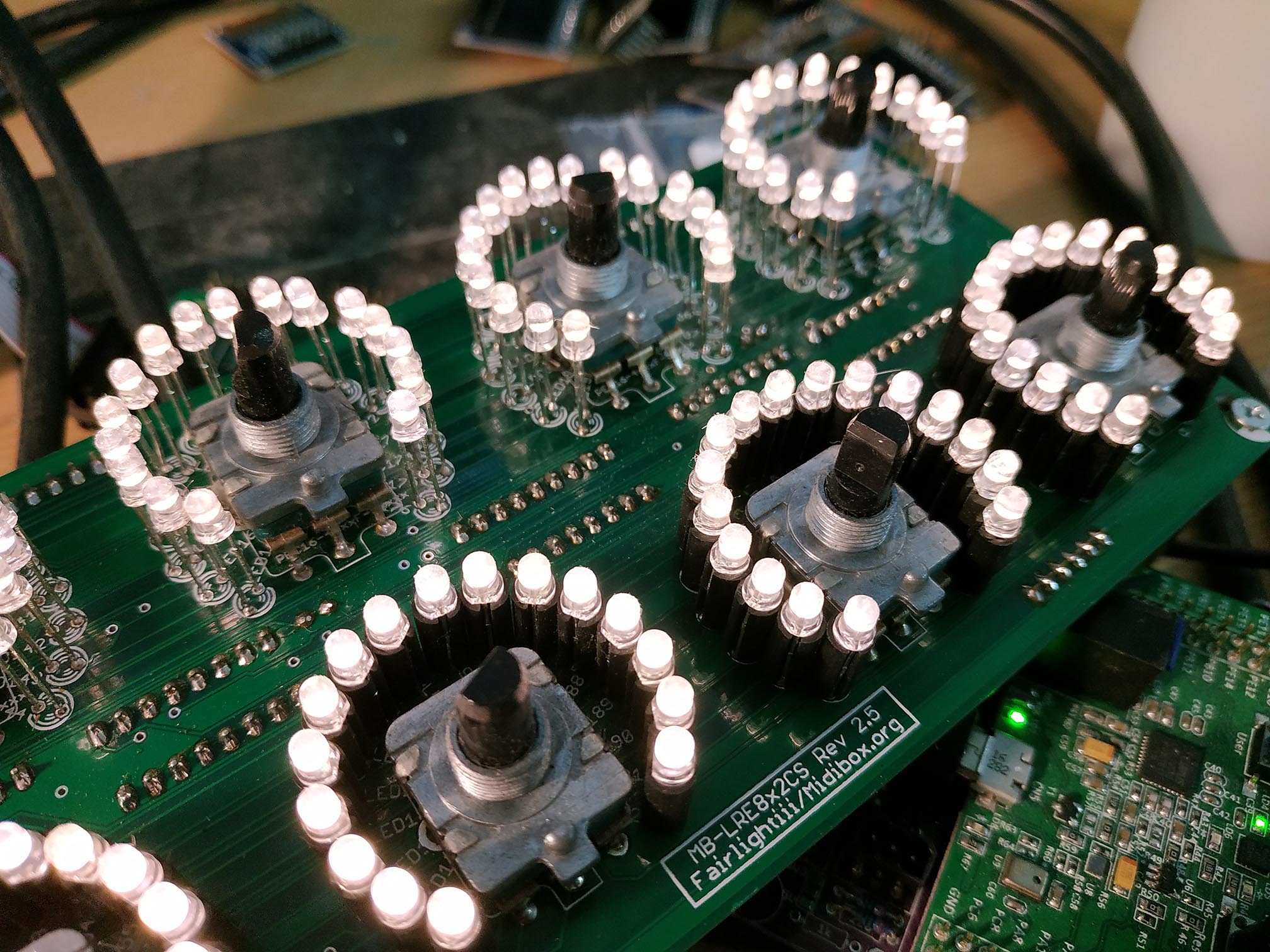
Next is a LRE:

It has warmwhite LEDs. Lower row is mounted on spacer, the others not. Encoders are PEC16 with integrated switches.
On the switch-header I soldered a flat-cable directly. So if you don't need it you have to remove it.Price: 35€
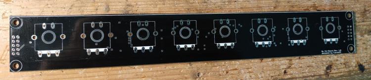
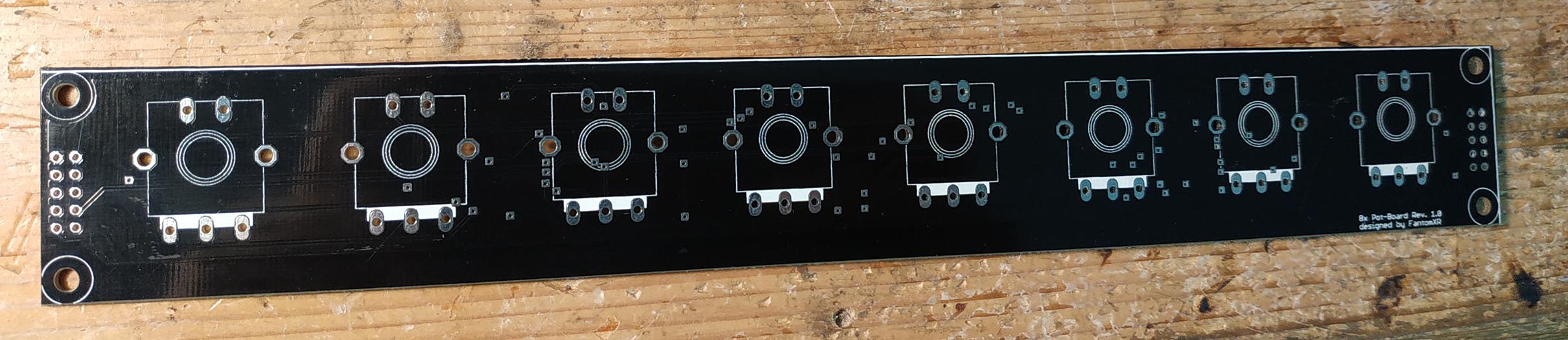
This is PCB where you can mount encoders on the top. Necessary shiftregisters have to be mounted on the backside. It's SMD, but can be soldered with a good soldering iron without any problems. No need for SMD-equipment like reflow-oven.
Price: 3€ each

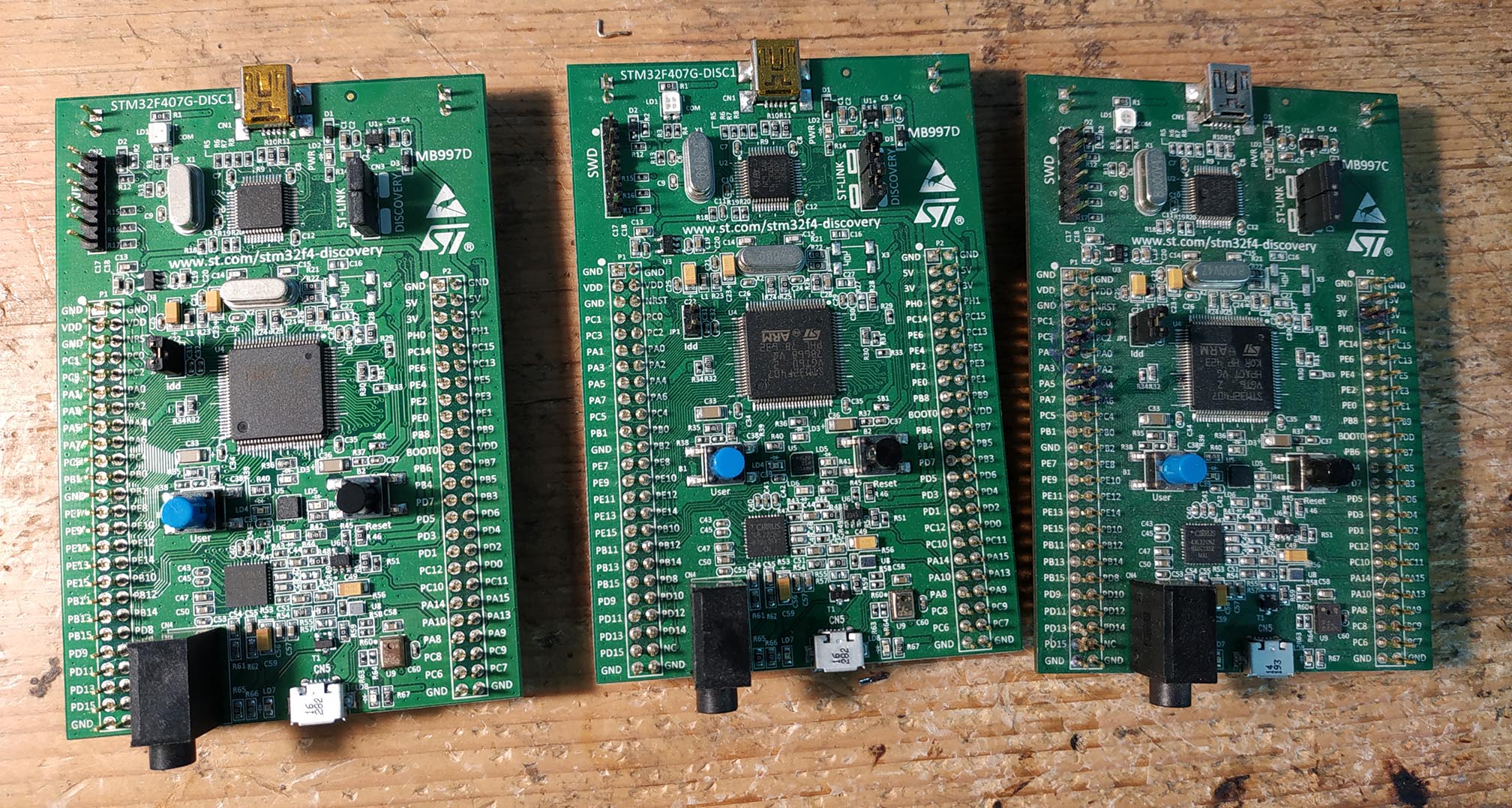
STM32F4 Discovery!
Price: 15€ each
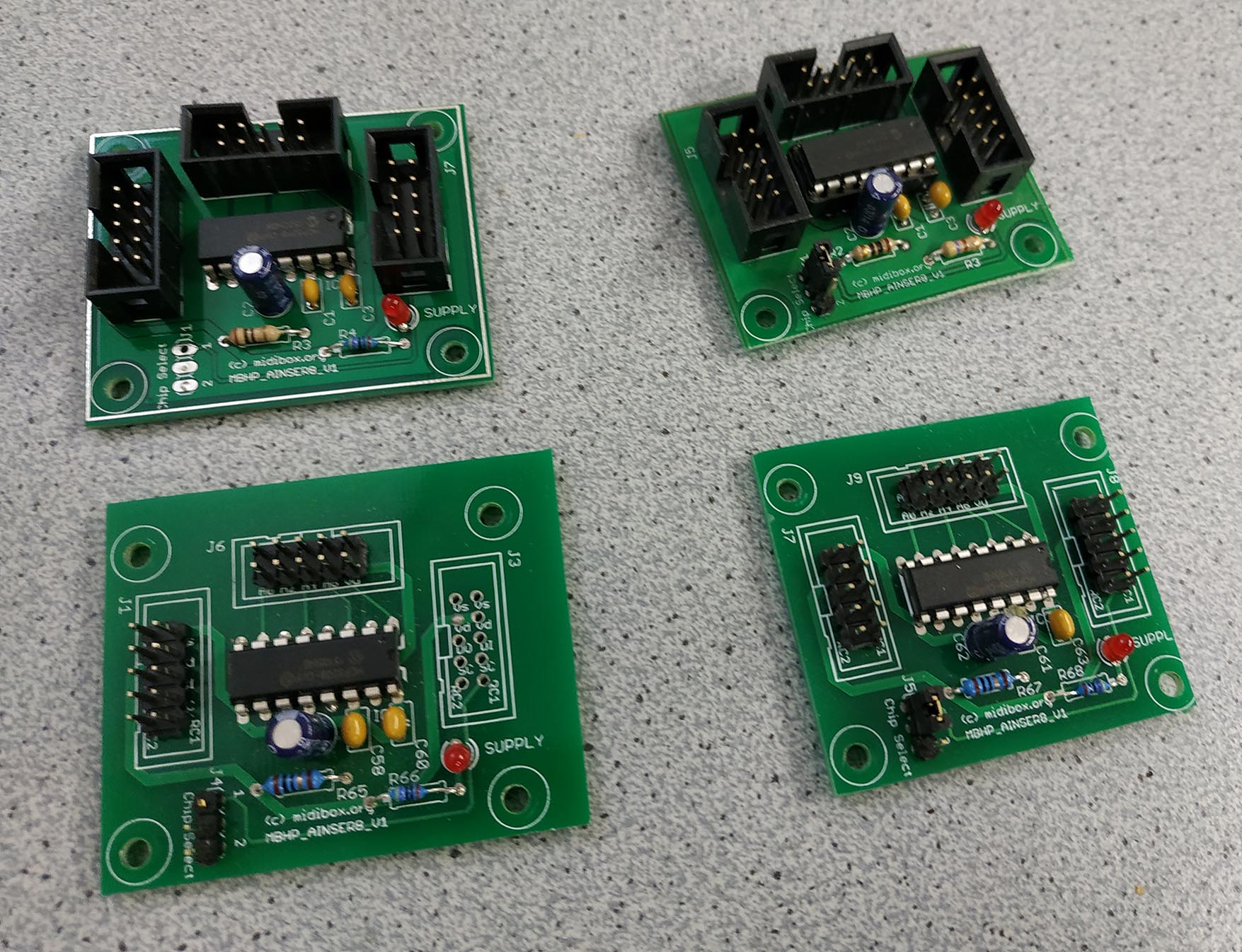
AINSER8-module assembled.
Price: 6€ each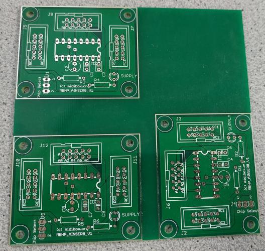
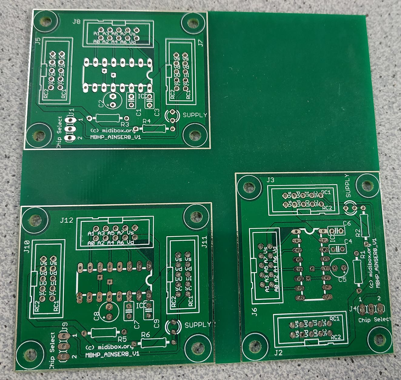
AINSER8-PCBs. Each PCB includes three layouts. I will not cut those in pieces. You have to do it by yourself.
Price: 4€ each PCB (=> 3 AINSER8 Layouts)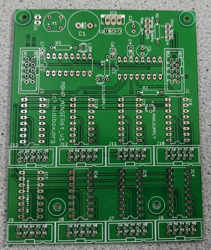
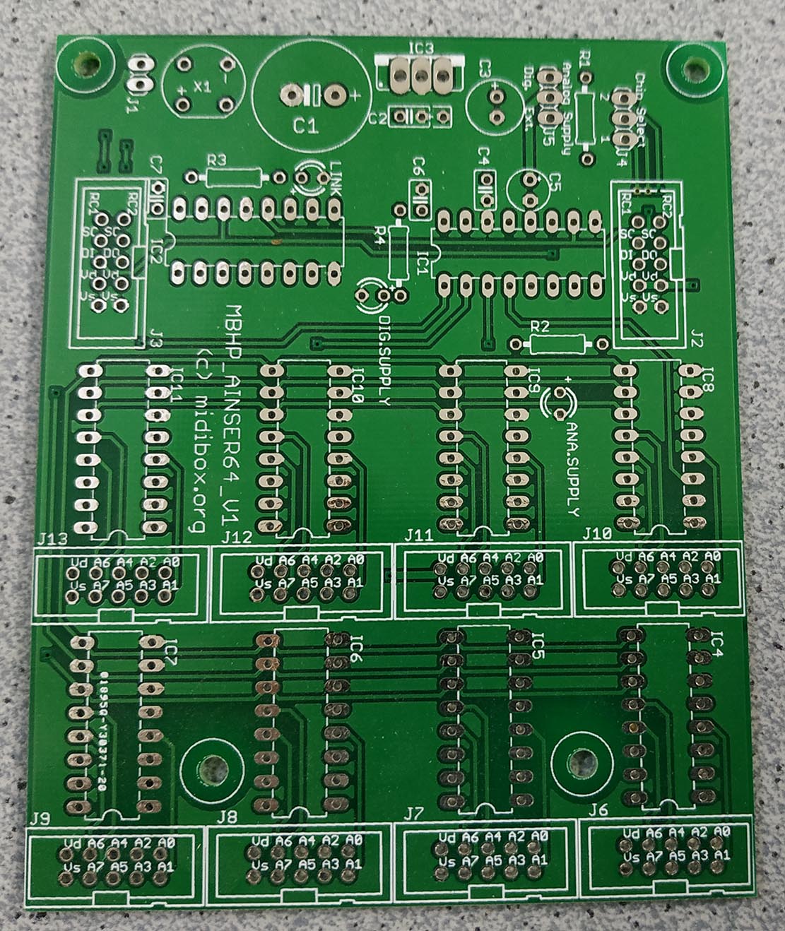
AINSER64-PCB
Price: 5€ each (two available)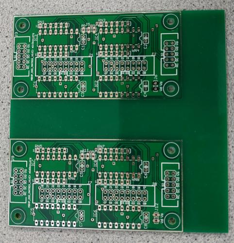
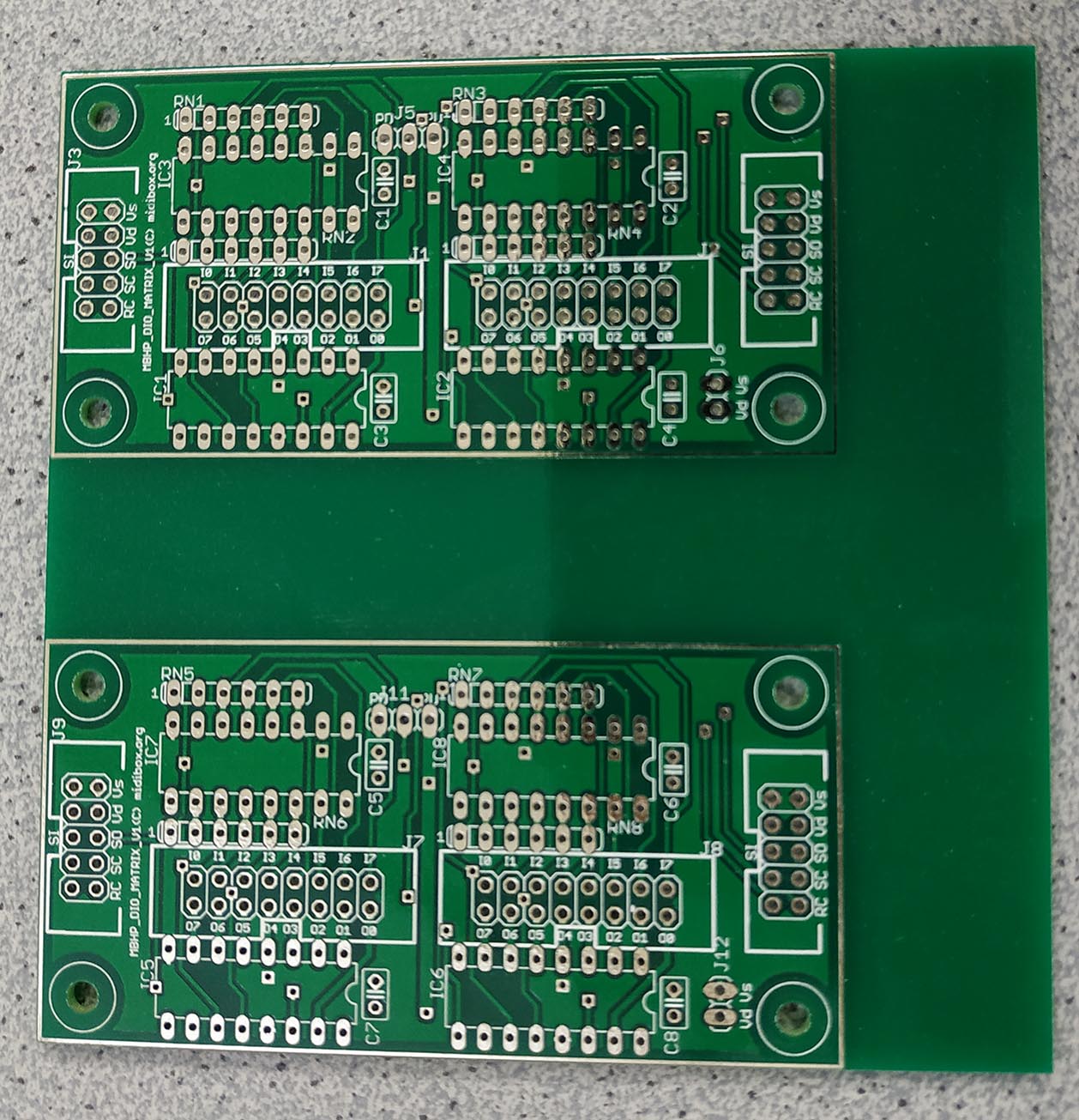
DIO-Matrix-PCBs. Each PCB includes two layouts. I will not cut those in pieces. You have to do it by yourself.
Price: 4€ each PCB (=> 2 DIO-Matrix Layouts).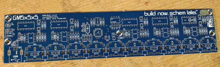
GM5x5x5-PCB
Price: 5€That's it for now!
I'm located in Berlin, Germany.Best,
Chris


Adding CS-line to AINSER8
in MIDIbox NG
Posted
Hi Zam! Thanks for your reply.
I've tried that without success.
Yes. I prefer having more traces (=not muxed) instead of having less traces and more parts (=muxed). I want to get rid of HC595 and 4051.
In my application I need about 20 analog inputs. So, unfortunately 16ch. are not enough.
I thought that too. But I comment out those lines. Also I did a double check I took these lines from mios32_spi.h:
#define MIOS32_SPI2_RCLK1_PORT GPIOA // RC1 #define MIOS32_SPI2_RCLK1_PIN GPIO_Pin_15 #define MIOS32_SPI2_RCLK1_AF { GPIO_PinAFConfig(GPIOA, GPIO_PinSource15, GPIO_AF_SPI3); } // only relevant for slave mode #define MIOS32_SPI2_RCLK2_PORT GPIOB // RC2 #define MIOS32_SPI2_RCLK2_PIN GPIO_Pin_8 #define MIOS32_SPI2_RCLK2_AF { } #define MIOS32_SPI2_RCLK3_PORT GPIOC // RC3 #define MIOS32_SPI2_RCLK3_PIN GPIO_Pin_1 #define MIOS32_SPI2_RCLK3_AF { }and changed the pin for RC1 to PC1 like this:
#define MIOS32_SPI2_RCLK1_PORT GPIOC // RC1
#define MIOS32_SPI2_RCLK1_PIN  GPIO_Pin_1
#define MIOS32_SPI2_RCLK1_AF   { GPIO_PinAFConfig(GPIOC, GPIO_PinSource1, GPIO_AF_SPI3); } // only relevant for slave mode
#define MIOS32_SPI2_RCLK2_PORT GPIOB // RC2
#define MIOS32_SPI2_RCLK2_PIN  GPIO_Pin_8
#define MIOS32_SPI2_RCLK2_AF   { }
#define MIOS32_SPI2_RCLK3_PORT GPIOC // RC3
#define MIOS32_SPI2_RCLK3_PIN  GPIO_Pin_1
#define MIOS32_SPI2_RCLK3_AF   { }
And this is working great (of course with cs=0 in the NGC-file). So I don't think that PC1 is somehow "blocked" for this application.
It can't be to hard to add more CS. I think I just overlook something...