greevous
-
Posts
24 -
Joined
-
Last visited
Content Type
Profiles
Forums
Blogs
Gallery
Everything posted by greevous
-
Anyone tried using this? Any idea how you'd implement the lower level functions for bankstick?
-
Hi everyone, I was wondering if anybody has built any kind of basic file system for Bankstick? I've got 8 64k eeproms, and I'd like to treat them like a 512k drive without worrying about which chip I'm storing something on -- just a name and a block of data. Such an algorithm would have to deal with data crossing 64k boundaries on a chip, and would ideally acquire data 64 bytes at a time (the largest block supported in one read). Thoughts? Joe R.
-
FYI, I got my new TLV5630 (I got two of them for $7 each [5 euros] on ebay!) I installed it, and at first I was disappointed because I wasn't getting anything out of the DAC outputs, but I switched to the 3.3v mode, removed the R32 resistor network, and moved the J26 jumper to 3.3v, and everything started working as expected! So, probably I can't drive at 5v because of the crappy cables I'm using (Where can I get cheap headers, sockets, and ribbon cable? I'd like to make all this stuff nice and professional.) I'm so happy now. I can now move forward with building my minimoog keyboard emulator! Thanks TK for helping me debug the original problem (bad TLV5630).
-
Well, for the record, I removed C10 and let the REF pin float and tried running again. It did not work -- everything was the same. So, I ordered a new TLV5630IDW. Any advice on how to install it without frying it again? Do I need some kind of special heat sink to keep the solder pen's heat out of the chip? I don't know if I fried it with heat, fried it with static electricity, or fried it with a short circuit, but my guess would be heat. Oh, also, for the record, after I decided to order a new DAC, I changed the CTRL0 control byte in aout.c so that it was switched to external reference (making the REF pin an input pin), and connected it to +5v (the data sheet says you can drive it all the way to AVdd, which is what I did). For the five working channels, it did indeed push them up to around 4.6v (AVdd-0.4, just like the datasheet says), which allowed me to use the op amps to push the outputs close to 10v. However, the first three channels still didn't work. I put the outputs on a scope, and noticed they were oscillating a bit (more as the voltage got close to max). So, presumably I'd need to add a cap to the REF line and ground it or something to get rid of the oscillation. However, running in that configuration, the DAC became warm to the touch (not hot, but uncomfortably warm) after a few minutes, so I decided this hack wasn't worth using. I'll just put a new DAC in, but I did want to document for posterity that external referencing does appear to work. Since I'm replacing the DAC anyway, and need to wait for it to arrive, I may throw a cap on the reference line just to see if I can get rid of the oscillation in the output channels (maybe the oscillation was the cause of the heat, not sure). That way people would know that this is a viable configuration if they chose to do it.
-
It looks like in the datasheet for the TLV5630 that the output channels range from 0 to 2X REF, so I guess the 5 channels that are running are working as expected (REF = 1.13v and they're putting out around 2.22v when sent 64000 == 4000 in 12bits). The issue seems to be that the REF (pin 16) is stuck at 1.13v and we can't get it to take the CTRL0 command to use an internal reference of 2v, which is what the following should produce, correct? // 00001000 << 4 == 1000XXXX (CTRL0 address) MIOS32_SPI_TransferByte(AOUT_SPI, 0x8 << 4); // 00000001 << 3 | 00000011 << 1 = 00001000 | 00000110 = XXX01110 (DOUT Enable + Ref Set to 2v Internal) MIOS32_SPI_TransferByte(AOUT_SPI, ctrl0); Maybe replace C10? The schematic shows it should be 100nf. I'll see if I've got another one. I really need to get that REF up to 2v so that 2X2 gets me to 4v output, which in turn could get stretched to approx. 10v by the op amps. I don't need all 8 channels, 5 would be ok, but I gotta get up to 10v on the outputs. Maybe I'll replace C10 and see what happens. Alternatively I could buy another TLV5630, but I'm not sure how to get the old one off the board. I'm disappointed that I apparently fried the DAC somehow. Maybe we need an AOUT LC with a multi-channel S&H IC? Oh well, I'll replace the cap and see what happens.
-
Ok, all jumpers and op amps pulled: pin #1: 0.00v pin #2: 0.49v pin #3: 0.32v pin #4: 2.97v pin #5: 5.41v pin #6: 2.22v pin #7: 2.22v pin #8: 2.22v pin #9: 2.21v pin#10: 0.00v pin#11: 5.41v pin#12: 0.01v pin#13: 0.01v pin#14: 0.02v pin#15: 2.09v pin#16: 1.13v pin#17: 5.41v pin#18: 0.00v pin#19: 0.49v pin#20: 5.41v
-
I reset J26 back to 5v and put #define AOUT_SPI_OUTPUTS_OD 1 back in (went back to the original code). status |= MIOS32_SPI_TransferModeInit(AOUT_SPI, MIOS32_SPI_MODE_CLK0_PHASE1, MIOS32_SPI_PRESCALER_4); pin 16 = 1.05v status |= MIOS32_SPI_TransferModeInit(AOUT_SPI, MIOS32_SPI_MODE_CLK1_PHASE0, MIOS32_SPI_PRESCALER_4); pin 16 = 1.05v status |= MIOS32_SPI_TransferModeInit(AOUT_SPI, MIOS32_SPI_MODE_CLK1_PHASE1, MIOS32_SPI_PRESCALER_4); pin 16 = 1.05v ...doesn't seem to make any difference in pin 16.
-
Ok, I will try these in an hour or so (having breakfast) and report back!
-
Alright, I switched the #define AOUT_SPI_OUTPUTS_OD 0 setting (it was in \modules\aout\aout.h), pulled the resistor network from R32, and moved J26 to 3.3v, recompiled my code, pushed it to the core, and measured everything on the TLV5630 after flipping the switch, which sends 64000 to all 8 channels. This is the voltage of every pin on the TLV5630 after sending the 64000: #1: 0.00v #2: 0.02v #3: 0.02v #4: 3.49v #5: 3.49v #6: 1.95v #7: 1.95v #8: 1.95v #9: 1.95v #10: 0.00v #11: 3.47v #12: 0.01v #13: 0.01v #14: 0.02v #15: 1.75v #16: 0.99v #17: 3.47v #18: 0.00v #19: 0.00v #20: 3.47v So I think it is still acting the same way at the 3.3v setting. I can see the clock pulses on pin 5 of J1 when data is being sent. I do know that: AOUT_IF_Init(0) returns -4. The documentation says < 0 means the call failed, but I think that might be bogus, because it's returning -4 because 255 is coming back from: status |= MIOS32_SPI_TransferByte(AOUT_SPI, 0x8 << 4); and TK said that 255 was a normal return code for MIOS32_SPI_TransferByte() Thoughts?
-
Ok. I'll go do that right now. I wasn't sure if you wanted me to move ahead with your suggestions because there was some confusion on what I was seeing on the pins of the DAC (that's why I created the PDF, to make sure I knew exactly what was happening). I'll let you know what happens soon.
-
I'm not sure how to read the datasheet, but it appears that there are two different modes that the TLV5630 can go into, and one of them runs at 2v on pin 16, and the other runs at 1v on pin 16. Apparently there's some kind of control register you write to to change modes. I'm guessing this is what the AOUT_*_Init() code is supposed to do. Maybe there's a bug in it for the TLV5630 running as I have it configured? I did stumble across this code. Someone apparently wrote a driver for the TLV5630 that presumably would be similar to the one in MIOS32 (not sure if it's bit banging). I may try to compare them and see if I can see any difference (one difference I noticed already was that the NutDac driver asks for communication speed when doing its initialization -- I'm going to see if I can figure out what it does with this parameter). Any ideas from TK or anyone else would be greatly appreciated.
-
Ok, to eliminate confusion, I decided to take voltage measurements and put them on a picture (attached PDF). As you can see, pin 16 is floating around 1.04v (TK, you said it should be approx. 2v I believe). Also, as you can see, 5 of the 8 output channels are putting out around 2v, and three of them are putting out almost nothing (OUTA, OUTB, and OUTC). The code that's driving this simply sends 64000 (defined as a u16 variable) to all eight channels when a switch is flipped. I can flip the switch back and forth, and the 5 channels that are working go back and forth between 0v and 2v as measured on the TLV5630. I don't understand why I'm only getting 1v at pin 16. Also, if I'm nearly maxing the data inputs (64000), shouldn't the output channels on the TLV5630 be close to 5v instead of 2v? Any idea why OUTA, OUTB, and OUTC don't seem to change value and stay close to 0v? I have not tried any of your suggestions yet. I wanted to give you this information to see if it told you something I'm doing wrong. AOUT_NG.pdf
-
Thorsten, I see +1.05v on pin 16. I also realized that output channels 4,5,6,7,and 8 are actually working, sort of. When I send 64,000 on those channels, they raise to about +5.7v, and are close to +0v when I send 0. For some reason the first three channels (the ones I was testing) don't change from 0v. Why am I only getting 5.7v instead of approx. 12v on those working channels? I am guessing the three dead channels are burned up in the tlv5630 or something. I have not tried your other ideas yet.
-
Does anybody have a known working AOUT NG and STM32 J19 style cable they'd be willing to sell me? I don't seem to be getting anywhere with mine. I think my DAC must be blown -- nothing shows up on the outputs even though I see data streaming in on the inputs (I have no idea if the data is formatted right, but I have no reason to assume it's not). Maybe I fried it when I was soldering it in. It was the first time I soldered an SMD, and although the pins look good under a magnifying glass, maybe I fried it.
-
Could you please describe, how you are testing the AOUT_NG module exactly. I put my oscilloscope on the output channel pins, and it doesn't change when I turn my encoder (the encoder wheel just increments or decrements a counter that is fed to the AOUT). I thought maybe it might be a problem in my code, so I just wrote a very simple app that increments a counter from 0 to 65000 and feeds the value to all 8 channels and does an AOUT_Update(). I can see the three SPI pins sending lots of data when I do that, but nothing shows up at the output channels. Where do you measure voltages? Did you already try to measure the unamplified voltages directly on the TLV5630 pins? I did check both -- I checked the OUTA, OUTB, OUTC, etc. pins of the TLV5630, and none of them change -- they all sit close to ground. I checked all the GND and VCC pins going into the DAC, and they all seem normal. I also checked the three SPI pins and they match the J1 pins. Which pull-up resistor network are you using at J19 (J32), maybe it could make sense to try another value, e.g. 4*1k instead of 4*10k (or vice versa) The resistor network came with the kit from SmashTV... it's marked "5X-1-102LF". When I check pin 1 to any other pin, it measures approximately 1k. Jumper J26 of the core module is selected for 5V? (the resulting voltage on SC/RC1/SO pins should be ca. 4.4V) J26 is definitely on 5v. I'll load up the MBSEQ v4 and double check the voltages, but I think they are around 4.4v.
-
Ok, I got this: ------------------------------------------------------------------------------- Application successfully built for: Processor: STM32F103RE Family: STM32F10x Board: MBHP_CORE_STM32 LCD: clcd ------------------------------------------------------------------------------- arm-none-eabi-size project_build/project.elf text data bss dec hex filename 44976 96 12608 57680 e150 project_build/project.elf So, that probably means this is not a software issue, and is probably a hardware issue. I did add some delays in the \mios32\STM32F10x\mios32_spi.c (MIOS32_SPI_TransferByte) function inside the SPI software emulation code under the MIOS32_SPI_MODE_CLK0_PHASE0 switch/case, and I when I do that I can see the SC pin going high and low on my oscilloscope. I did notice that "in_data" always ends up being 255, no matter what data is being sent. Is that normal? I don't quite understand the macros that are being executed, so I don't know if that's normal. So, to recap, I pretty much know I have some kind of hardware issue, but I'm not sure what I need to do next. I tried a different cable and got the same behavior. Is my DAC dead? I'm afraid I don't really understand the SPI protocol well enough to understand what I should be seeing coming into and going out of the TLV5630. Maybe I should switch to my AOUT LC module just to split the hardware problem in half -- if it works with the AOUT LC module, then I know it's the AOUT NG module that's the problem. TK, I really do appreciate your help thus far. This is turning out to be a lot trickier than I planned.
-
Could someone with a known good STM32 tool chain compile my app.c above (the .h header is just stolen from one of the tutorials) and the #16 aout tutorial and then email the .hex files to me? jrounceville at hotmail.com I need to split the problem in half, either its my tool chain or my hardware. I didn't see pre-built versions of the #16 tutorial anywhere, otherwise I would have used that.
-
...but it's a bit confusing that the colours are a different on the pictures... Only the red wire is different (changes to brown because I had to splice it)... I should have mentioned that when I uploaded the pictures. I forgot about it. The SC pulses are very short, sometimes ca. 100 nS (= 5 MHz) Did you select the right timescale on your scope? I'm not sure. I'll double check the timescale. It would be interesting if you can see the pulses if the cable on the SC line is disconnected from the MBHP_CORE_STM32 module. Maybe the cable is too long? (what is the cable length?) The cable is about 20 cm long. I've measured both from the J19 interface on the core, and the J1 interface on the AOUT NG... both show nothing for SC unless I use the MBSEQ tool to force SC high or low. Note that J19 is a software emulated SPI port. This means, that if MBSEQ can control the pins, MIOS32_SPI should be able to do this as well without reconfiguring the IO pin. Are you using the prebuilt binary (beta44), or did you build the application by yourself? Did you already ensure that you are using the latest sources of the repository, and that you are not using modified sources? I built the apps using the source trunk, which I checked out about two weeks ago and refreshed last night to get the MBSEQ stuff. Maybe my toolchain is screwed up in some way? This seems doubtful though -- everything compiles fine. Maybe I need to dig into the source code of MBSEQ v4. Obviously MBSEQ's testaoutpin code is able to drive all three pins on and off by command, so there must be some difference between what it does when it's driving them manually vs. when I use AOUT_PinSet(). I wish I had a multichannel oscilloscope... I'd like to watch all three at the same time... If I can't get J19 working, is it possible to use J8? I'm currently using J9 for a DIN interface, but my understanding is that J8 is a hardware SPI interface?
-
I forgot to mention that this whole exercise is to get a high quality MIOS32/DAC combo that is going to be used to drive the keyboard and left-hand-controller circuits for my Minimoog clone: http://sites.google.com/site/minimoogwiki/ I already had it "sort of" working with a MIOS8 and an AOUT LC, but that was too limited because I couldn't fit all the code in it and needed more output channels to drive the left-hand-controller circuit (I'm replacing the original left hand controller and the keyboard with a MIOS solution so I can use my minimoog clone with the rest of my synth rig [Roland Junu-G, Roland JV-30, Roland JX8P, Korg Microkorg]).
-
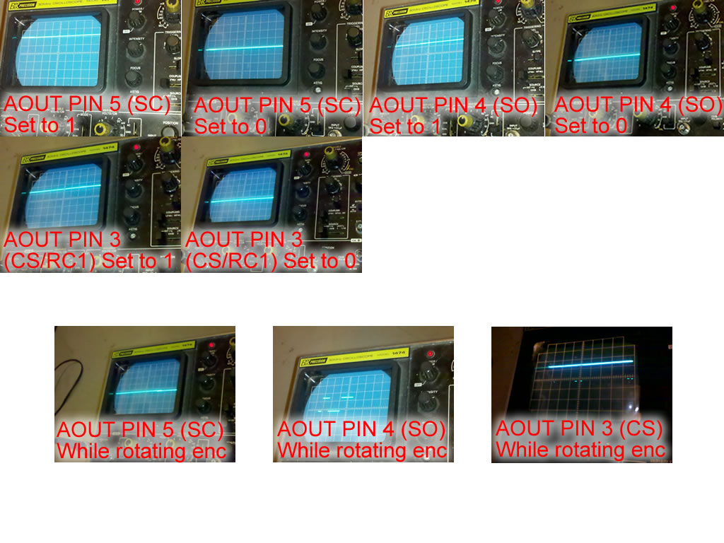
I've created a PNG that shows my oscilloscope on all three serial pins (the vd and vs are normal). First I show myself manipulating them with the MBSEQ tool (demonstrating that they work). Then, I show all three while I'm sending data to the AOUT. You'll notice the SC doesn't seem to do anything while I'm rotating the encoder. I've attached my test code as well, in case this is some kind of software problem (although I don't think it is, because I don't get anything out of any of the output channels of the AOUT NG with Tutorial #16 when sending data from my synth via midi -- I see the MIDI messages in the console, but nothing from the AOUT NG outputs). app.c
-
Here's a couple of photos. I hooked up my oscilloscope to each pin and watched its behavior. When I use the testaoutpin thing in MBSEQ, I can toggle each pin up or down as you would expect. However, when I use the AOUT Tutorial #16 with my midi keyboard, the SC pin never moves off of GND. When I use my little test program (which just sends a 16 bit counter value to channels 1, 2, and 3), I see the same thing -- the SC pin doesn't move off of GND. The other two serial pins seem to be doing something. one of them looks sort of like (where the _ is actually very tiny) ------_--_-------_--_-------_--_ and the other one looks sort of like --------___---------_________--__ but the SC pin looks like _________________________________ I looked at the datasheet for the DAC, and I guess I would expect the SC pin to look like this, correct? _-_-_-_-_-_-_-_-_-_-_-_-_-_-_-_- Any help would be appreciated. Should I try switching to the second set of pins in the J19 block? I don't understand why I can set SC just fine with the MBSEQ tool, but when I use anything that actually sets the value through the normal API, SC doesn't seem to do anything.


-
I installed the MBSEQ program, and used the testaoutpin functions, which definitely showed a +4 / 0 thing happening on each pin when I told it to (although I noticed that they varied a little -- one pin was around 5v and another was around 4 when turned on), but I'm not getting anything out of the output channels. Any ideas how I should debug?
-
Well, I got those wires switched as they should be, but I'm not getting anything out of any of the output channels on the AOUT NG. I checked the Op Amps, and they're definitely getting their V+ and V- as they should. Can I load the MBSEQ .hex even if my setup doesn't include all the hardware for the MBSEQ? Basically I've got a single chip DIN module, and AOUT NG module, and a single CLCD module. I hooked a scope up to J2, and I definitely have Vd, Vs, and a pin that seems to strobe low when I rotate my encoder. Is that the clock line? I'm sort of a newbie to this and I don't really know how to debug from here. When I built my AOUT LC, it just worked, so I didn't need to debug anything. This time I didn't get so lucky I guess.
-
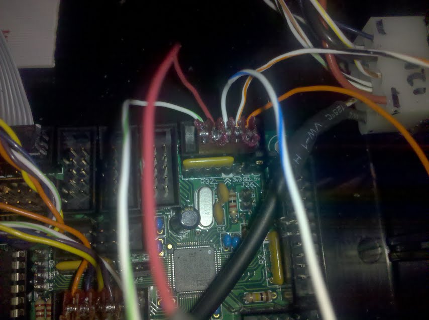
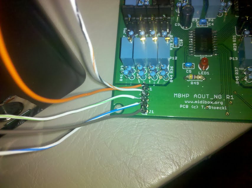
Can someone tell me the proper way for J1 to be connected to the STM32 core? I've got it connected to J19 (RC1 side), and I think I've got all the pins figured out except #5. J1.1 = GND (Vs on core J19) J1.2 = +5v (Vd on core J19) J1.3 = Frame Sync (SO on core J19?) J1.4 = Digital Serial Input (RC1 on core J19?) J1.5 = Serial Clock Input (SC on core J19?) I'm beginning to think my assignment for J1.3 is wrong... maybe J1.4 should be SO on core J19, and J1.3 should be RC1? Then what is J1.5, SC on the core? Since "SO, SC, and RC1" don't really match to the pins of the DAC or the pins of the STM32 itself, it's a little confusing. Right now I'm getting nothing but a slightly glitchy fixed voltage out of all 8 channels of the AOUT NG, but I think it's because I'm not driving the DAC properly due to confusion on the J1 interface. The only pins I know for sure are right are GND and +5v.