
This N°9
-
Posts
331 -
Joined
-
Last visited
Content Type
Profiles
Forums
Blogs
Gallery
Posts posted by This N°9
-
-
blm-module ?
http://svnmios.midibox.org/listing.php?repname=svn.mios&path=%2Ftrunk%2Fmodules%2Fblm%2F
I never used it, and it's for duo, not RGB LED's, and written in asm. From your code I guess your are not targeting mios32. There are two BLM-modules for mios32:
http://svnmios.midibox.org/listing.php?repname=svn.mios32&path=%2Ftrunk%2Fmodules%2Fblm%2F
http://svnmios.midibox.org/listing.php?repname=svn.mios32&path=%2Ftrunk%2Fmodules%2Fblm_x%2F
Maybe you could find some inspiration there, or port parts of the code for your application.
-
hi protofuse,
is there a special reason why you don't use an existing blm-module for your application? I did not study your code / postings in deep, just flew over it.
-
I updated fairchild about the condradicting answers, and provided a link to this forum thread ca. a week ago.
Now they marked the request as "solved" without further comments, so do I. You can read all the answers, numbers, test results in this thead. Make yourself a picture and decide yourself.
My personal opinion:
it is possible to drive 8 LED's at max. 20mA each with one 74HC595, without damaging the IC, but I won't recommend to go beyond 20mA * 8. The advantages of using additional drivers are: less power consumption (less heat dissipation), more stable current supply (without: current drift max. 4.5% @ 8*20mA).
-
....the influence between outputs....
I did some more test to have a clear answer to this:
74HCH9H, 220R at each output:
- one pin through 220R to ground: Isingle = 19.9mA
- all eight pin's to ground, single pin current I = 19mA --> Itotal = 152mA
Max. current drift @ ca. 20mA (max) each output: 4.5%
This is acceptable, you will hardly see a visible change when switching on 1 or 8 LED's.
I also measured the voltage drops:
- one pin through 220R to ground : Udropsingle = 0.6V
- all pin's through 220R to ground : Udroptotal = 0.61V
With those numbers I could calculate:
- The total power dissipation when all pin's are sourcing ca. 19mA:
Ptot = Udroptotal * Itotal = 92.7mW
- Assuming a simplified model of the current flow through a common resistor, and the single drivers (simplified to constant resistors in parallel), I could calculate the common resistance, through which all the current of all drivers has to flow, and the resistance of the single driver (only @ ca. 19-20mA each output!):
Vcc---Rcommon----Rdriver---- Out 1
¦
¦
-- Rdriver---- Out 2
¦
..
..
Isingle = 19.9mA (current for a single pin sourcing)
Itotal = 152mA (current for all pins sourcing)
Udropsingle = 0.6V (Vdrop from Vcc to a single output sourcing)
Udroptotal = 0.61V (Vdrop from Vcc to outputs when all pin's are sourcing)
Rsingle = Udropsingle / Isingle = 30.15R
Rtotal = Udroptotal / Itotal = 4.013R
Rsingle = Rcommon + Rdriver -----> Rcommon = Rsingle - Rdriver
Rtotal = Rcommon + Rdriver / 8 ---> Rcommon = Rtotal - Rdriver / 8
Rsingle - Rdriver = Rtotal - Rdriver / 8
7/8 * Rdriver = Rsingle - Rtotal
Rdriver = ( Rsingle - Rtotal ) * 8/7 = (30.15R - 4.013R) * 8/7 = 29.8..R
Rcommon = Rsingle - Rdriver = 30.15R - 29.8..R = 0.35R
Power dissipation at the common resistor (Vcc-pin, bond-wire, and the common way on the silicon to the supplies of the single drivers) if all pins sourcing:
Udropcommon = Udroptotal * (Rcommon / Rtotal) = 0.053..V
Pcommon = Udropcommonres * Itotal = 0.053V * 152mA = 8.09..mW
Power dissipation of a single driver (all outputs sourcing 19mA each):
Pdriver = (Ptot - Pcommon) / 8 = ( 92.7mW - 8.09..mW ) / 8 = 10.57mW
-
You have to differ between how much current can a 74HC595 source/sink w/o the risk for damage, and how much current can a single 74HC595 output source/sink w/o influencing the current through other outputs (resp. w/o violating the logic-level specs, but this isn't for interest here anyhow).
That's exactly my point of view too. In my tests, where I sourced 33mA from each output (which is not necessary in LED applications, as a LED should not be driven beyond 20mA, regardless of colour), I measured a voltage drop of 1.46V from Vcc to output pins. Of course this violates logic level specs, but LED's don't care about logic levels.
1.46V * 264mA -> power dissipation 385.44 mW (uppper limit is specified beyond 600/750mW, depends on manufacturer), so I guess the chip will not be damaged under those conditions.
On my original 4x16 Duo-LED Matrix design, there is a noticable influence once more than 8 LEDs are sinked through a single 74HC595 at the same time. Therefore I recommented sink drivers.Note that I never planed to sink that much current directly through 74HC595. With a current of 12mA each LED (this is a fact when driving LED's with 74HC595 & 220R resistors), you would have a sink current of 96mA. This is simply not possible, the datasheets specify a sink limit for a sinlge pin of 20mA. Even when grounding a high pin, you will have only a current of 68mA. I guess this will be aboout the same for sink current, I never tested this, because it's not interesting for my application. For sinking, I use the ULN2803, they are cheap and I just need one even for a huge matrix. The driver chips I found are more expensive, and complicate the whole design, and I would need several chips for a matrix. So I would like to use the 74HC595's directly just for sourcing.
Comment to answer from Fairchild: they are right - they are speaking about a current limit through a single pin, they don't mention the influence between outputs, but you haven't asked for this...This is not totally correct. My exact question was, if it is possible to source 20mA each output simultaniously without damaging the device. My original question to fairchild:
Is it possible to draw 20mA each output pin (at the same time) from the 74HC595? My aim is to drive LED's.I read in the datasheet "DC VCC or GND Current, per pin (ICC)", this indicates that 20mA each output will exceed this limit, or is this value per driver / logic unit?
I did some tests regarding input/output current with the 74HC595, which aproved that the 74HC595 is able to provide this source, but I don't know if it will get damaged under those conditions.
The whole discussion thread can be found here: https://fairchildsemi.custhelp.com/cgi-bin/fairchildsemi.cfg/php/enduser/myq_idp.php?p_sid=l7MUBgxj&p_accessibility=0&p_redirect=&p_lva=&p_sp=&p_li=&p_iid=77963&p_created=1241624385&p_allorg=1
Comment to answer from ON: they are right, but Voh/Vol isn't for interest while driving LEDs (in other words: miss-using a logic chip)Yes, true. My only concern is, if 20mA each output simultanously will damage the device. Of course it's an abuse of the original usage aim of the chip, but if it works and does not damage the IC, I don't care :)
To make more clear what my aim is: if it's possible to source 20mA per output (simultanously), and ..
- ..this way of driving the LED's will not affect brightnes if one/several LED's are on (which seems to be not a problem, as I alredy drive the LED matrix like this)..
- ..will not damage the chip..
- ..will not make the input logic (registers / latches) unreliable..
..this would be the most easy/cheap way to drive the matrix.
In either case (special source drivers or not), I'll use the ULN2803 for sinking.
-
I got the answers from ST,ON and fairchild:
ST:
Dear customer,the mentioned current is for the complete IC. If you like to drive LEDs, plese refer to the product selector on our website under:
Here you will find a list of our LED driver Portfolio.
Best regards
fairchild:
I am not sure what is the other manufacturer part that you use for your application, but what my opinion is if the part is the cross reference of Fairchild part, then it should be the same of current limit per pin.
ON:
This part is not capable of sourcing or sinking much more than approximately 10 ma. The Voh and Vol specifications list 7.8 ma at a Vcc of 6 V. We do not have a logic IC that is capable of a 35 ma output. You need to consider other parts such as Mosfet drivers. -
I am currently torturing our little friend 74HC595 a bit more, to let it talk about it's current drive capabilities, as I have still no answers from tech supports at fairchild, ST micro and ON providing contradicting information:
condition: total output current = 270mA (33.75mA each output)
after ca. 10min:
temperature: 41° C (surrounding air ca. 21° C)
voltage drop Vcc->output terminals: 1.46V
this results is a power dissipation of 394mW, well below 500mW (consolidated max. rating different manufactueres)
-
I started a new discussion on sparkfun's forum. I think "max. power dissipation" could be the magic word(s):
http://forum.sparkfun.com/viewtopic.php?p=72352#72352
basicly, if you multiply the voltage drop from Vcc to the drivers, at a given output-current each driver, with the total current Vcc-> drivers, you get ca. the power dissipation, as the input's and logic do not need a lot of current. At 20mA each output, I measured a V-drop of ca. 0.75V -> 120mW Pd, upper limit is 500/600/750 in plastic DIP, depending on manufacturer. 1° C / 10mW is the temperature derating, the device got 36° C @ 8x20mA. makes sense at a room temperature of 20-25°C.
As the out-driver's resistance is no constant and will raise at raising current, 35mA source current per output makes sense in the context of max Pd.
EDIT: in other words, if the IC does not overheat, I see no reason why it should get damaged
-
Basically that means that there are different types of 595s out there
Are you sure? I beleive there are common specifications for 74HC logic family types. My assumtions is that ON and other manufacturer just missed the "per pin / logic unit" information in their specs. Besides my tests don't include fairchild devices, and the results look more like the answer from fairchild would make more sense. When 70mA is really the limit for the whole device, there must be a bottleneck somewhere, this can only be the bond wire or a common Vcc / GND line on the silicon. This would show either in a current cutof @ 5V when you reach some current value, or the device would get very hot. Both is not the case, even if I drive *a lot* more current than 20x8 mA (see test results in my first posting).
These are all speculations so far, I fed this info back to ON, and hope their answer will clear the issue. I will also ask fairchild if their per-pin spec just covers their own devices. I think this is safer than rely on speculations.
-
Funny, fairchild semi gives a different answer (the one I wanted :D ):
Replied By: MH EngResponse: Hi Matthias,
The max rate of DC output current and the DC Vcc and GND current is only for one pin.
Thus, if the DC Vcc current per pin is 70mA max, so 8 X 70mA = 0.56A ( max ). In your application, there are only 12mA per pin, 96mA would not damage the part.
I beleive each register unit will have it's own bond wire to the Vcc/GND terminal, so the only part that has to take the total current is the pin / terminal itself.
So, happy news, it's possible to source/sink the full current rated for one pin (25mA sink, 35mA source).
-
Sorry that I may fall on your nerves by beeing so sticky to this.. but if a current > 70mA would really be a condition that could damage the 74HC595, then the standard MIDIbox solution for driving LED's would be in serious troubles.
I really don't beleive that this is the case, as somebody until now would have noticed this, and my 74HC595 experiments go far beyond the 12, even far beyond 20mA per pin, and the device is still alive.
Ok, I did not test for hours or days, but even at 200mA supply current, which is a case that will never be used to drive LED's or additional logic devices, the 74HC595 did not get warmer than 53° C after ca. 10min.
I assume that the maximum rating is to ensure a proper logic-1 level of 5V at the outputs, that's not relevant when driving LED's. At 20mA at 7 outputs, the voltage of the 8th output drops to 4.86V (Vcc=4.93V), maybe this could cause instable contitions for some logic families (bad slew rates etcetc.). The device does not overheat or something, and I don't thing that the bond wire will melt under those conditions, and the current specs of the single outputs will not be violated, so what?
Because I'am very stubborn, I also contacted fairchild semicondutor's support. They have a very nice knowledge base & asking-questions site (not this we-want-to-sell-but-we-don't exist-thing), where you can get a member and ask questions. I'am waiting for the answer from there now.
Besides, some people in the arduino community also use exactly the same approach (74HC595 + 220R) to drive LED's : http://www.arduino.cc/en/Tutorial/ShiftOut (But you have alway to be careful with those DIY punks.. :) )
-
My head is always shaking really fast. Crack + coffee == bad combohe word is "duty cycle" - did you ever shake your head quickly while looking at a MB? the LEDs are only on part of the time so the average current is lower than calculated. If you're interested in numbers, you should ask TK.
seppoman, it must have been the crack + coffe.. set a dout-pin to high, take a scope, connect it to the pin, watch your scope and turn the time/div button from 1uS up to 1mS, you will always see a straight horizontal line (don't shake your head while doing it).
Why should there be a duty cycle? The 74HC595 have latches, which hold the logic 1 until the data is shifted from the core to the registers. Latch enable will transfer the content of the registers to the latches, there's no time when the pin will be low.
Of course, if you have a multiplexed solution, there you have the duty cycle, but normally if you just want to connect some, say 16, LED's, you will do no multiplexing. So you will have a constant current from each output to the LED of 12mA (aproved by measuring it with 220R at outputs). 12x8 = 96, this is quite more than 70mA -> violation of the maximum ratings (if the technical assisten of ON tells the truth, assumed he has a clue and not just reads the datasheet too).
-
the word is "duty cycle" - did you ever shake your head quickly while looking at a MB? the LEDs are only on part of the time so the average current is lower than calculated. If you're interested in numbers, you should ask TK.
Duty cycle with standard DOUT's (no multiplexing)??? 12mA is exactly the current that I measures flowing through a LED connected to DOUT with 220R. If there would be a duty cycle, I would measure a lower value with a normal multimeter. And if you look at the tests I did, you see that the 74HC595 will not cut off at total current > 70mA. I scope will show the truth this evening..
Is it possible that the 70mA limit is only to guarantee a proper logic 1 level, and not to prevent the chip from damage? I wonder because:
I connected all the pins set to high through 220R to ground, and measured the sum current from all pins to ground: Ipins-gnd : 142mA (!)Then I let the 74HC595 in this state for some minutes, and measured the temperature: 36° C (free air).
The voltage Vcc came down to 4.8V
-
I contacted ON Semiconductor to get the definitive (?) answer:
Thank you for contacting ON Semiconductor.The DC supply current listed in the maximum ratings is valid for whole device. Output current per pin is allowed to be max 35mA, but this is not for all pins at the same time, but just for one or two so the total current will not exceed 75 mA. Of course this is maximum rating and it is not recommended to use these limit values for standard operation of the device.
Indeed distrelec.com gives me a different / no answer (translated from german):
Thanks for your request.We are sorry, we also just can try to interpret the datasheets / give an understandable translation:
..
"Supply Current" is the Current measured at the IC Supply terminal per Logic-Unit
Wanted to know what "Logic-Unit" refers to (translated from german and cooked down to the basic message):
Sorry we can't give you a definitive answer, so please refer the datasheet.
I love datasheets.
So what about 8xLED @ 12mA (with 220R at SR outputs) > 70mA ?
-
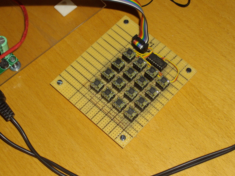
After finishing the coding of the blm_x driver to drive a button-LED matrix, I was doing a lot of experiments to learn about the best way to drive it. My aim is to drive a soft-button matrix from sparkfun.com with RGB LED's. On the way some question marks passed my way, one of it was:
How much current is a 74HC595 able to supply? I read the datasheet(s), and had some problems to find the right interpretation of the numbers I found there:
Clamp Diode Current (IIK, IOK) ±20 mA
DC Output Current, per pin (IOUT) ±35 mA
DC VCC or GND Current, [glow=red,2,300]per pin[/glow] (ICC) ±70 mA
Phillips uses diffrent labels for the numbers:
input diode current ±20 mA
output diode current ±20 mA
output source or sink current
Q7’ standard output ±25 mA
Qn bus driver outputs ±35 mA
VCC or GND current ±70 mA
It looks like the 70mA is the max. sum current the 74HC595 can supply. There was a discussion about that in the programmers lounge (private access), I decided to continue it here. Some of the quotes from the discussion there:
TK:
A single 74HC595 output usually doesn't source more than 25 mA.This:
The 70mA is not the max. current that the 595 can provide, but the shortcut-current (shorting a pin to gnd/Vcc). 35mA is the max. output-current, and 20mA (output clamp current) seems to be the current that can be fed in the 595 per pin (when pin is low). In one datasheet this value was clearly labeled as input current. The last I read from fairchild makes the 70mA-value more clear (per pin!):Clamp Diode Current (IIK, IOK) ±20 mA
DC Output Current, per pin (IOUT) ±35 mA
DC VCC or GND Current, [glow=red,2,300]per pin[/glow] (ICC) ±70 mA
seppoman:
for me, this reads as "the 70mA IS the max. continuous current that either the GND pin or the VCC pin can carry - this can be partitioned to one or several pins, but a single pin can only carry 35mA max" i.e. as soon as all 8 are on, each can only take about 9mA. I agree the wording in different datasheets can be a bit fuzzy at times.stryd_one:
Due to the mass confusion about this spec, SmashTV was kind enough to sacrifice a SR some time ago, and the results confirm that you are correct.this:
Something's on my mind: if I connect 8 standard red LED's (Vf 2V, If 20mA -> 100R) through a 220R resistor array, the output current of a single pin will be ca. 5V/(100+220+142)R = 10.8mA142R would be the output resistance of a single pin if the max. output current is 35mA. It could be even less(?). But 10.8 * 8 = 86.4, this is above the speced 70mA. I never noticed a change of brightnes when all LED's connected to a SR are turned on, but when these numbers are correct, the current would fall if the max. 70mA are reached, or the 595 would be in stressed state. Can somebody help me to understand this?
So, because of all this confuction, I did some experiments with the 74HC595 myself. Here are the results:
- Grounding a single output pin set to high (no resistor, other pins open): Ipin = 68mA
- Connecting a single output pin through 220R to ground (other pins open): Ipin = 20mA
- Connecting a LED through 220R (other pin's open): Ipin = 12mA
The next test result looks very interesting to me:
I connected all the pins set to high through 220R to ground, and measured the sum current from all pins to ground: Ipins-gnd : 142mA (!)
Then I let the 74HC595 in this state for some minutes, and measured the temperature: 36° C (free air).
The voltage Vcc came down to 4.8V
The results show: the 74HC595 is able to have a current of 142mA through Vcc without getting very hot or something, and all the pins are able to provide ca. 17mA at the same time (with 220R resistors)! But I just wonder for how long, and if the device will get damaged.
The other question mark that struck me: when I connect 8 LED's to a SR with 220R resistors (the standard MIDIBox solution to connect LED's), the total current through Vcc of the 74HC595 will be ca. 96mA.
This is more than the specified 70mA max. I really wonder about this number, especially because I read a shortcut-current of 68mA when grounding a single pin. This is suspiciously near to the 70mA. And: "DC VCC or GND Current, per pin (ICC) ±70 mA", why should they write "per pin" if this number would simply refers the max. current that can enter the Vcc terminal? Maybe it's rather the max. current that can flow from the Vcc terminal to a single driver! (?) And 35mA is the max. current that should leave a output terminal without stressing the driver to much? After all the experiments and datashits this would be the explanation that looks the most reasonable to me.
Why I'am so interested in this?
- I worry about my (and all the other) midiboxes driving eight LED's simultaniously :D
- I want to know if I can drive my RGB LED's without having additional drivers at the source side.
I need ca 19mA for the red color to match with green / blue (they'r much brighter)
Maybe somebody can give me some comments and help me ease the pain in my brain?
EDIT:
some more test results:
- Ground 3 pins (no resistors), read current of fourth pin -> ground: I = 55mA
Temperature of 74HC595: 45° C
- Ground 4 pins (no resistors), read current of fifth pin: 51mA
Temperature of 74HC595: 53° C
But still alive.. 5 pins grounded sums up to a total current of 255mA. Here it starts to look critical to me. Now multiply 35mA with 8, you get 280mA.. the max. output current rating. 55° is still acceptable, now put the device in a closed box, and it will start getting critical. Does this make sense or not?
After all this I'm quite sure the 74HC595 can source 8 pins with 20mA each without any problems. What do you think?
-
along the way i ran into two errors when i run make in a clean copy of the sdcc_skeleton from svn
I suppose you first made a clean checkout of the whole mios-repository?
did you define your environment variables properly? in my kubuntu system:
MIOS_PATH="/home/this/mios/trunk"
MIOS_BIN_PATH="/home/this/mios/trunk/bin"
MIOS_SHELL="/bin/bash"
I added those lines in "/etc/environment" to have them set at startup automatically. You should not have to modify mios-gpasm at all, this looks like some basic missconfiguration to me.
If you have your toolchain set up properly (sdcc / gputils), and the environment variables above, try "make" in the sdcc skelleton folder. If this fails, there's something wrong.
If this works, copy "main.c" "Makefile" "README.txt" from the sdcc skelleton folder to a new folder (without .svn dir!) and start coding :-)
-
Oh thats nice! MIOS32 will support 1MHz IIC natively. As soon as I have the STM32 (and checkd it out a bit), I'll try to port the FRAM module.
I also made some benchmark tests with the FRAM:
subsequent block writes/reads, 16KBytes in one chunk, repeated 16 times (4xFM24C512) (address just sent once at the begining):
fast mode:
write 256KBytes: ca. 2.9Sec
read 256KBytes: ca. 2.7Sec
This is a bit faster (if I calculated right) than your benchmark, but I suppose it's because I only (need to) send the device- and memory-address once for 16KBytes transfer.
I really could go to the edge of the timing maximum ratings and noticed no problems so far with a ca. 15cm long cable. The big advantages of the FRAM is the write-speed and the endurance (1 billion r/w cycles). Drawbacks are the price (ca. 10euro for a FM24C512), and they are only available as SMD.
Current state: mios_iic / fram_iic@1MHZ successfully tested over J4. Builded a board stuffed with a 4-channel analog multiplexer and 16xFM24C256 -> 1MB. The default setup (for PIC) will be: RC4/RC5 SCL/SDA; RD5/RD6 multiplexing. Everything can connect with one single ribbon cable.
I'am currently trying to run tests with the multiplexed version, but I have some problems. Maybe I have to add pull-up's, or it's something else.. I'll find out.
Once things will work completly, I'll create a wiki-page for the module and give some more info there.
by the way: aatis.de sells these little SMD adapter for a very modest price. I don't know if they ship only to europe or also overseas:
http://www.bausatz.aatis.de/SO2DIP_SMD-Adapter/body_so2dip_smd-adapter.html
EDIT: just read the spec again, output of the device is open-drain. So I add pull-ups. This also has the advantage, that if the wiring is incorrect, NAK will be read by default. The good thing about this: because I missed the pull-ups, I found a bug in the code (high-level read returns zero if the last byte read was a 0x00, that's defined as error-response) :D
-
The label before 'udata' can be used for banksels.
I see. A UDATA section will always entirely reside in one bank. Also good to know!
EDIT: http://www.midibox.org/dokuwiki/doku.php?id=home:software:picasm
-
so, here are the results of my UDATA/RES research. I tested different solutions and the effect they have. I added the resulting addresses as comment to the labels (@stryd: this is also the proof that labels without RES are NOT the same as with RES 0):
FRAM_VARS UDATA
FRAM_REG ; 0x000088
_FRAM_REG RES 1 ;0x000088
FRAM_ERROR ;0x00008a
_FRAM_ERROR RES 1; 0x000089
this is not really the intended result. don't do thisFRAM_VARS_1 UDATA FRAM_REG ;0x00008a _FRAM_REG RES 1 ;0x00008a FRAM_VARS_2 UDATA FRAM_ERROR ;0x00008b _FRAM_ERROR RES 1;0x00008b
the addresses look good and are unique, but it has some strange effect on the codespace. For example the display will not switch to the second line, the constant 0x40 in codespace seems to get fucked up. Don't do this either!FRAM_VARS UDATA _FRAM_REG RES 0 ;0x000088 FRAM_REG RES 1 ;0x000088 _FRAM_ERROR RES 0 ;0x000089 FRAM_ERROR RES 1 ;0x000089
this seems to be the proper way to define two labels at the same memory position. The addesses are correct, unique and the program behaves like it should. and to end the story: <label 1> RES 0 has always to be *before* <label 1> RES X ! else the RES-0-Label will obtain an address, but no meory will be reserved for it:FRAM_VARS UDATA FRAM_REG RES 1;0x000088 _FRAM_REG RES 0;0x000089 FRAM_ERROR RES 10x000089 _FRAM_ERROR RES 00x00008a
so the valid way to have identical variable names in C/ASM is:
vars_x UDATA
_var1 RES 0
var 1 RES 1
_var2 RES 0
var2 RES 1
now I'am satisfied with this :D
-
I think that what is happening here is that the res directive persists for following lines. I guess that makes it a bit less typing, because you can do:
I'am not quite sure about that... when you look at the first example I provided in the first post, you can see a quite strange behaviour. And besides, a field that I defined globally in C only, will have the same address as one of my ASM fileds. So it seems that with the label without RES directive, the assembler will give the label an address, but not really reserve the memory location. That's why it will be used again:
FRAM_VARS UDATA
FRAM_REG RES 1 ;0x000088
_FRAM_REG ;0x00008a
FRAM_ERROR RES 1 ;0x000089
_FRAM_ERROR ;0x00008c
_address 0x00008a data extern _output/main__mios-gpasm-tmp.asm
'address' is I field that I defined globally on application level then. As you can see it has the same address as FRAM_REG. So the assembler seems to increment the memory address pointer (in the module), but it will not reserve the address, the linker uses the same address in the application (main.o) again. Maybe a label in a UDATA section without any directive equals a shared field. This would make sense.
anyway, the only thing I wanted is not to have the ugly _ vars in the ASM code.. Maybe I have to be a bit less aestheticly fanatic and have a working software instead :)
by the way.. my 'solution' for having two labels at the same memory address is not confirmed to work as intended. I have strange behaviours in my app since I changed it this way (LCD not switching to second line, wrong increments etc.).
I'll study the gputils manual again, and do some more test. You may say that this is loss of time, but when I once touched this issue, I want to know what's going on! ;)
I will post any results here.
-
I found a solution that works:
FRAM_REG_ UDATA
_FRAM_REG
FRAM_REG RES 1


FRAM_ERROR_	UDATA
_FRAM_ERROR
FRAM_ERROR RES 1
now the addresses look better to me.. :_FRAM_REG 0x00008a data extern /home/this/mios/trunk/modules/fram/fram.asm FRAM_REG 0x00008a data extern /home/this/mios/trunk/modules/fram/fram.asm _FRAM_ERROR 0x00008b data extern /home/this/mios/trunk/modules/fram/fram.asm FRAM_ERROR 0x00008b data extern /home/this/mios/trunk/modules/fram/fram.asm _address 0x000088 data extern _output/main__mios-gpasm-tmp.asm
What is the label before 'udata' even for? It seems that I can't use it in my code as a memory address. Are there other(better) ways to define two labels on the same memory address, like I can do in codespace?
-
hi,
I had some strange bugs, which at the end showed up as overlapping variables:
FRAM_VARS UDATA
FRAM_REG RES 1
_FRAM_REG
FRAM_ERROR RES 1
_FRAM_ERROR
gives me this:FRAM_REG 0x000088 data extern /home/this/mios/trunk/modules/fram/fram.asm _FRAM_REG 0x00008a data extern /home/this/mios/trunk/modules/fram/fram.asm FRAM_ERROR 0x000089 data extern /home/this/mios/trunk/modules/fram/fram.asm _FRAM_ERROR 0x00008c data extern /home/this/mios/trunk/modules/fram/fram.asm
and this oneFRAM_VARS UDATA _FRAM_REG FRAM_REG RES 1 _FRAM_ERROR FRAM_ERROR RES 1
will be that_FRAM_REG 0x000088 data extern /home/this/mios/trunk/modules/fram/fram.asm FRAM_REG 0x000088 data extern /home/this/mios/trunk/modules/fram/fram.asm _FRAM_ERROR 0x00008a data extern /home/this/mios/trunk/modules/fram/fram.asm FRAM_ERROR 0x000089 data extern /home/this/mios/trunk/modules/fram/fram.asm
can somebody explain me shortly what the **** is going on here? labels in data space seem to behave quite differently. the reason why I even got suspicious, was that the error-code seemed to match the address LSB! :_address 0x00008a data extern _output/main__mios-gpasm-tmp.asm
I will use separate UDATA sections for each C/ASM variable instead now, but I wonder anyway what is going on here. no warnings or so at all... my intension was (obviously) to have the ASM/C variable at the same address, and I also had the idea that it shouldn't be shared with other variables :D
-
thanks.
looking at the MIOS Pin List, I found a little "bug":
"RD4 / E / J10:SO" instead of "RD4 / E / J14"
and in the description of RA4 there should be mentioned that also MIOS_Bankstick_* functions use the PIN. Same for RD5 "clock output to bankstick" -> "clock output to bankstick / IIC".
-
J4.SD is exclusively used by the IIC handler, while J4.SC is available on the LCD and J10 (application specific) port as well. This port is used by MIDIbox SID for example, according to the pin list, it's a class H pin
So calls to MIOS_LCD_xxx and any IIC-related functions are not save during a FRAM-session. Which are the functions/modules that use the IIC port (besides MIOS_Bankstick_xxx and MIOS_IIC_xxx)? I just would like to document this in README.txt of the module.
I guess the ISR will never manipulate any of these PINs (J4 SD/SC and J10 SO/RC), even not in applications like SID?
but I guess that you will support a "safe mode" for mapping to shared pins anyhowI first decided not to do this, because this will allocate additional code space. But on the other hand it's just some instructions that would have to be called in the app if there's no save-mode-functions. Anyhow, the ability to do subsequent reads/writes and to handle data between two read/write calls is a big advantage, so I would like to have a good documentation about what can be done in a FRAM session and what not.
Forum Login Problem
in Latest News
Posted
I can't login to the forum the normal way, I always have to use the "frogot password function.." When I try to log in with the new reset password, it doesn't work.
Somebody else has this issue?