robinfawell
-
Posts
292 -
Joined
-
Last visited
Content Type
Profiles
Forums
Blogs
Gallery
Everything posted by robinfawell
-
SRIO, DOUT, DIN, 16 bit , 8bit Confusion
robinfawell replied to robinfawell's topic in MIOS programming (C)
Dear Duggle You are right. I wasn't thinking straight. All cables are flat cables with IDC 10 pin plugs. The cable from the Core to the DIN module is about 4 inches. The cable to the DOUT module is daisy chained from the output of the DIN module and is about 2 inches. This is probably not ideal. It may be better to make one cable with a core 10 pin IDC plug with two connectors at the other end, one for the DIN and one for the DOUT. This would reduce overall length. It would also mean that the signal paths from core to module would be more equal. If equal lengths the 10 pin cable could be split using a crimped terminals at the DIN / DOUT end. I agree that we should see how far we get using standard modules before adding additional components . Robin -
SRIO, DOUT, DIN, 16 bit , 8bit Confusion
robinfawell replied to robinfawell's topic in MIOS programming (C)
Hi Thorsten Two Switch Velocity Scanning I have analysed a method to control the sending of Midi On (with velocity) and Midi Off using a Truth Table. This method assumes that the 2nd Switch DIN Byte is read immediately after the 1st Switch DIN byte. I'm not sure whether the logic has flaws but it may be useful. Robin 1st Sw 2nd Switch same scan.doc -
SRIO, DOUT, DIN, 16 bit , 8bit Confusion
robinfawell replied to robinfawell's topic in MIOS programming (C)
Dear Thorsten I've attached a revised MIOS STUDIO debug report. I have checked this twice. I'm not sure what the delays mean. I have definitely shown the high velocity data followed by the low velocity data. I think that I have deleted the unwanted text>. Regards Robin The time between the 1st switch closing and the 2nd switch closing is what determines the velocity. Shorter time means higher velocity and vice versa. It is not a changeover switch. See the Fatar circuit I sent earlier ""matrix_88"" time stamp 2.txt -
SRIO, DOUT, DIN, 16 bit , 8bit Confusion
robinfawell replied to robinfawell's topic in MIOS programming (C)
Dear Duggle Thanks for your reply. Yes I do, but it is a fairly basic one. I haven't used it for some time. I will see if I've got a 10:1 probe for it. Yes I have 2 sets of both DINs and DOUTs. I've been reading Horowitz & Hill (Art of Electronics) they suggest the use of 100 ohms in series with 100 pf from DIN input to ground as an ac termination. I think I've also read that the DOUT impedance is in the order of 50 ohms. In my case there are also an unknown set of diodes with some non-linear impedance when DOUT is low. I will be pleased to try out anything you think will be beneficial to improve the waveforms. Regards Robin -
SRIO, DOUT, DIN, 16 bit , 8bit Confusion
robinfawell replied to robinfawell's topic in MIOS programming (C)
Dear Thorsten Your reply was very speedy. I have attached the time stamp data from MIOS STUDIO in a Notepad txt file. It shows 8 lines. The first 4 lines are for a high velocity press and the second four lines are for a very slow press. I have also checked all keys, I confirm that the Pin Nos are in line with my table. Best Regards Robin time stamp.txt -
SRIO, DOUT, DIN, 16 bit , 8bit Confusion
robinfawell replied to robinfawell's topic in MIOS programming (C)
Thanks Thorsten I've checked out the new fast scan program with MIOS Studio and the results are attached. The pin Nos are shown in Red. I've also checked out reducing the number of rows to 13 rather than 16. It works fine, as would be expected. In addition I've marked in Green the Note Nos. You will see that when the first key A0 is pressed that pin 1 closes followed by pin 2. The sequence of what happens is shown with an extract from MIOS Studio. When the key A0 is pressed the 1st switch of the A0 key closes (row 1,col 0, pin value = 0),the 2nd switch closes (row 2, col 0, Pin value = 0). When the key is released the 2nd switch returns to a pin value 1, followed by the 2nd returning to pin value 1 The exercise has shown the order in which the keyboard switches are scanned and is very useful. It has also helped me to better understand the programming methodology. For the final version, which will be velocity sensitive, I have always thought that the scan time should as small as possible and that DMA transfer would be needed to achieve this. I understand with the default settings and using DMA a 16 X 16 matrix can have a 220 microsecond scan time. From your scope measurements 400 microS is about twice this. Duggle discussed this in an earlier message to me. For a very soft key press 128 scans may be needed (if max resolution were to be achieved!). This would take 128 mS at 1mS per scan. Maybe this is too long? So far, with the 16 X16 matrix I have not seen any evidence of switch bounce using MIOS Studio. Another thought I have is to investigate "impedance matching" between the DOUT outputs and the DIN Inputs. Has any work been done on this? This might help in allowing higher frequency clocks. Perhaps some of Duggle' recent work on chaining shift registers may give some pointers. Thanks Again Robin PS Towards the end of Fast scan 16 X 16 there is a STATUS line. What is this for? // read DIN, write DOUT s32 status = 0; u8 din0 = MIOS32_SPI_TransferByte(MIOS32_SRIO_SPI, (select_row_pattern >> 8) & 0xff); u8 din1 = MIOS32_SPI_TransferByte(MIOS32_SRIO_SPI, (select_row_pattern >> 0) & 0xff); Row Col Fast Scan A.doc -
SRIO, DOUT, DIN, 16 bit , 8bit Confusion
robinfawell replied to robinfawell's topic in MIOS programming (C)
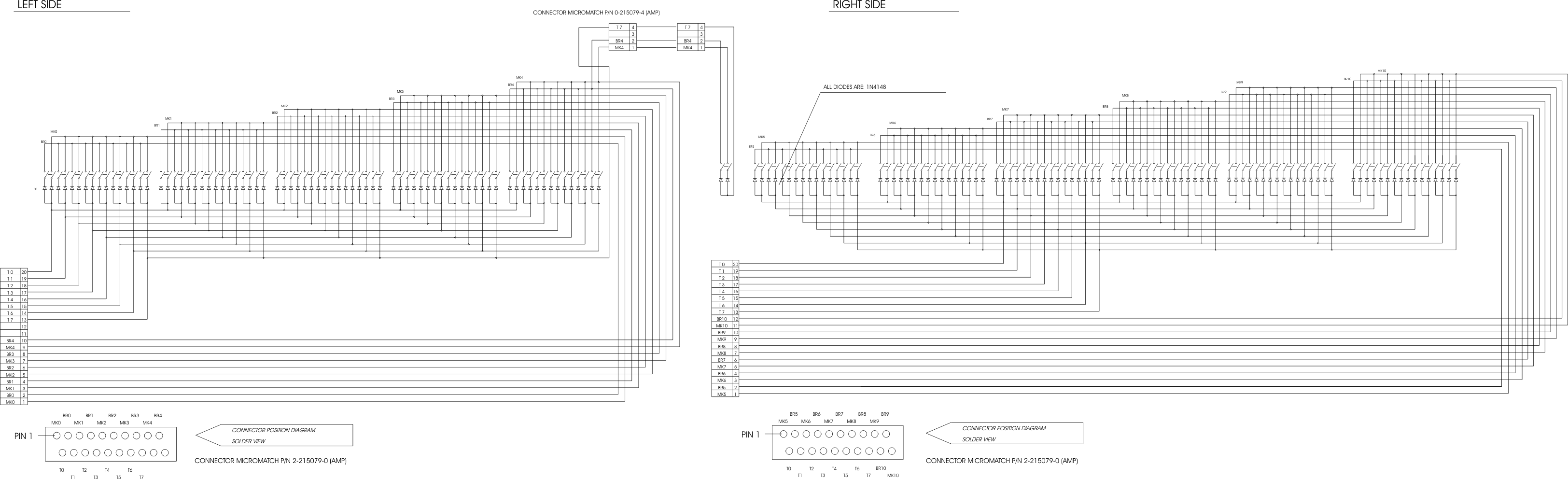
Thank you Thorsten. I have attached the drawing of the Fatar keyboard and the connections to DIN and DOUT. Matrix Board This shows that I have connected:- J3 DOUT Pin1 D0 to BR0 and BR5 J3 DOUT Pin2 D1 to MK0 and MK5 etc When a key is pressed BRx (1st switch) closes before MKx (2nd switch) closes. When the key is released MKx opens first followed by BRx. Fatar Circuit If you examine the arrangement you will see that I could have chosen a 22 DOUT X 8 DIN matrix. However there are restrictions on the length of SR's. Hence the choice of 16 X 16. On this point is a 12 X 16 matrix feasible? You can see that I have J4 DOUT D4 - D7 unused. The arrangement shown in the table is not sequential but I think that it may be the best compromise. The pin order and Midi Note will need to be adjusted. I can utilise the unused J4 DOUT D2 and D3 for the 2 piano pedals and for changing the Midi channels. I really appreciate your time in helping me. Regards Robin Fatar Midibox Matrix Board MIOS32D.doc
-
I have been reading and re-reading all the elements of the MIOS32 SVN Repository. Traditional Models, SPI, SRIO, DOUT, DIN. As mentioned previously I am building a digital piano. I want to use a 16 bit DIN and a 16 bit DOUT to scan the keyboard contacts. There are 2 X 88 switches to scan. s32 MIOS32_SRIO_ScanStart(void *_notify_hook) This function refers at the end to :- MIOS32_SPI_TransferBlock(MIOS32_SRIO_SPI, (u8 *)&mios32_srio_dout[0], (u8 *)&mios32_srio_din_buffer[0], MIOS32_SRIO_NUM_SR, MIOS32_SRIO_DMA_Callback); This shows the two buffers for DOUT and DIN as 8 bit (single bytes). Similarly in Din.c ///////////////////////////////////////////////////////////////////////////// //! Returns state of a DIN shift register //! \param[in] sr shift register number (0..15) //! \return 8bit value of shift register //! \return -1 if shift register not available ///////////////////////////////////////////////////////////////////////////// s32 MIOS32_DIN_SRGet(u32 sr) { // check if SR available if( sr >= MIOS32_SRIO_NUM_SR ) return -1; return mios32_srio_din[sr]; } The preamble shows that an 8bit value will be returned. Question 1 The DIN module reads 16 bits of data with each DOUT strobe. Can and how does MIOS32 deal with this in terms of 8bit values? Question 2 Has anyone written some code that would be helpful? Please help me in my confusion! Robin
-
The link does work! You will then see all the correspondence on this topic in the programmers lounge. Robin
-
That's good. Thanks niLS. Robin
-
-
I'm beginning to try out some code by modifying the srio example. I'm using the SVN Tortoise software. When I compile the various files show an error " ! ". I assume that this means that the system is warning me that there are changes. SVN is a read-only system! Reading the Wiki SVN Client Set-up for Windows document shows that PuTTY can be used. Is this the method I should use? Obviously I don't want to change any existing files, but is there a suitable section in the repository that I can use to try out my new code? Alternatively is there another way which would be more suitable for a relative C novice like me ? Robin
-
I have been trying out a few tutorial programs and the SRIO example. Everything was working OK but now I have a consistent error. Microsoft Windows XP [Version 5.1.2600] (C) Copyright 1985-2001 Microsoft Corp. E:\Documents and Settings\robin>cd mios32 The system cannot find the path specified. E:\Documents and Settings\robin>cd\ E:\>cd mios32 E:\MIOS32>cd trunk E:\MIOS32\trunk>cd apps E:\MIOS32\trunk\apps>cd examples E:\MIOS32\trunk\apps\examples>cd srio E:\MIOS32\trunk\apps\examples\srio>make E:\mios32\trunk/include/makefile/common.mk:123: *** multiple target patterns. S top. E:\MIOS32\trunk\apps\examples\srio> What would cause the multiple target patterns referred to ?
-
I believe that you only need 12 bits of DOUT ie 2 X DOUT chips. 11 bits might look possible. If you examine the table you will see that BR10 and MK10 are on the RH Fatar connector. You cannot drive both BR10 and MK10 with J4 DOUT D2 signal otherwise you will not be scanning. The Table shows that J3 DOUT will drive BR0 and BR5 together using signal D0, MK0 and MK5 with D1 and so on. J4 DOUT will drive the rest using D0-D3. If you accept this explanation you may understand why I am concerned with the order of scanning the contacts. However this can be discovered experimentally. Thorsten has made some comments about this in reply to an earlier question in a previous recent thread. He has suggested the following As you have indicated it is best to proceed more slowly and use ScanStart in its present form with 1ms period and get the project moving. Initially I plan to scan all the contacts without worrying about velocity, pin order. Then to scan all 1st contacts. Then 2nd contacts. Then worry about the scanning order. All of this using provided MIOS functions. Please let me know if you agree with my assertion regarding the No of DOUT's required. And thank you once again. Robin
-
Fatar Midibox Matrix Board MIOS32D.doc Dear Duggle, Thank you very much. The table has several errors. I had mixed up the Pin Nos both for DIN and DOUT. You were also right about BR operating before MK. I have checked this. The new table reflects this. The switches are as shown in the attached circuit of the Fatar 88 keyboard. The 1st Switch BR closes first. The 2nd switch MK closes with further depression of the key. Both switches are normally OC. Both switches are SC when the key is pressed. The terms BR and MK (Break and Make, I suppose) are misleading. I prefer 1st switch / 2nd switch. The MK and BR signal (from DOUT's) clamp the DIN inputs(T0-T15) to 0.6V,using the DIN input resistor and keyboard diode only when the DOUTs are low (0V). Yes there is only one connection to BR10 and MK10. Pins 19 and 20 are not connected to the Fatar LH 20 pin connector. The matrix covers groups of 8 contacts see the circuit. I hope that it is now clearer to you and me! Robin PS Luckily the J3 and J4 connections are wired up correctly. I have to change all the BR and MK wiring.the

-
Thanks again Duggle I have not been clear in my last message. I have attached the interconnection diagram between the keyboard and the 2 DIN's and the 2 DOUT's. There are 2 Fatar connectors (20 pin), 2 DOUT Connectors and 2 DIN connectors. MK0 and BR0 correspond to the lowest 8 notes, MK10 and BR10 to the highest 8 notes. I have chosen the pin allocations to preserve the natural order of the keys as much as possible. I have assumed that the 1st scan is J3 D0. This will give the 1st set of switches (MK0) data from the lowest 8 notes on J3DIN (D0-D7) and the 5th set of switches (MK5)data to (D0-D7) J4 DIN. The 2nd scan J3 D1 involves the 2nd switch data (BR0) from the 1st group of notes to J3 DIN and the 5th switch data (BR5) to J4 DIN. I am trying to figure out the order of the data storage. It makes sense that the sequence is MK0, MK5, BR0, BR5, MK1, MK6, BR1, BR6 etc etc. However this is an assumption. I will need to know this to generate the correct notes. The second question relates to the unused signals D4-D7 of J4 DOUT. I am guessing that defining the len parameter in term of SR stages (in my case 16) translates as 32 bytes. Maybe I could shorten the SR value to 12 to shorten the overall scan. This still leaves the unused 2 bytes J4 DOUT D2 and D3 for other purposes. I hope this a little clearer. Robin Fatar Midibox Matrix Board MIOS32.doc
-
I have attached a table showing the analysis of successive scans to determine the code for the electronic piano I am building. This relates to one piano note. The two switches are mechanically displaced to enable the velocity to be measured. This is not new information and is based on other peoples work. Once the 1st switch is made and the Xor becomes 1 the counter is set to say 127. Until the 2nd switch is closed and the Xor changes to 0 the count is decremented on each scan. At this point the Midi Note On is sent with the velocity parameter. The counter will also be stopped. The Midi Note Off will be generated when two successive scans produce zeros. Note that a flag is set to prevent spurious generation of Note Off signals. There may be flaws in the logic of this approach or it may be simplified. In any case please let me know. Regards Robin1st Sw 2nd Switch.doc
-
Thanks Duggle I agree that the Din and Dout functions are easier to understand. They will be easier to test than the SPI_Transfer_Block. However I think that for the final version I should use the above function as part of SRIO_ScanStart function. I am puzzled by the Transfer Block function. It looks a if it is transferring 8 bit data. I have a 16 bit X 16 bit SR. Does this mean that this will be transmitted as 32 bytes? Is each 16 bit Din divided into 8 bits? My switch scheme uses the full 16 bits for the DIN inputs and only 12 separate DOUT's. Is it possible to define the Len parameter to reflect this? If anyone can answer the above questions your help will be appreciated. Robin
-
The Fatar 88 key piano uses 176 switches. Two switches are used for each key. They are labelled MK (0-10) and BR(0-10), total 22 switches. They are used in matrix fashion with two sets of "strobes" labelled T0 - T7. My solution to dealing with the matrix is to connect the MK and BK signals to J3DOUT and J4DOUT (Only 4 outputs are used with J4DOUT) The LH keyboard signals T0-T7 are used as inputs to J3DIN and the RH ones to J4DIN. All 16 inputs are used. This means that we have a 16 bit word, one byte for the LH section and one byte for the RH section. S32 MIOS32_SPI_TransferBlock The function shows that 8 bit words can be transferred to or from the SR combination of DIN /DOUT. I have a few queries about this operation. 1) I assume that it transfers the LH byte followed by the RH byte ie the 1st 16 bit word. This followed by the 2nd 16 bit word and so on. Is this correct? 2) Each alternate 16 bit word MK need to be compared (using exclusive-or) with the subsequent MK scan and the same with the the BR scans. This means that two buffers will needed for MK (current and last) and two buffers for the BR scans. Is this feasible? 3) How would I test that the transfers are taking place? Has MIOS Studio any facilities for this type of testing? 4) I've looked fairly hard but I cannot find any examples of the use of SPI Transfer Block. Let me know where to find an example. The WebSVN shows an example entitled SRIO but although it refers to the SRIO operation is shows only encoder operations. 5) I'm not sure whether the function SPI Transfer Block automatically provides the shifting of the Dout strobe. What data should be entered in the "u8*send_buffer" parameter when used with DIN/DOUT? I will be very grateful for time spent in answering my queries. Thanks, Robin
-
Thanks again Duggle I am very impressed by the simplicity of your code to adjust for black and white key differing velocity. Here is the reference to the Doepfer keyboard controller. I raised the issue in Feb 2008 on the forum. See Page 13 of the manual. They use Wheel 1 to adjust the velocity parameter during POWER ON. I have no wheel in my setup and I see no point in introducing a pot just for this adjustment. Once the factor has been decided by experiment it can be fixed. My link I am still struggling to understand the MIOS32 spi and srio functions and it will be some time before I start with the code. However your code will be incorporated when I get to the later stages. Robin
-
Thank you Phil and Thorsten for your replies. I am very grateful to both of you for putting the GPIO (Parallel data) ideas for fast scan matrix into perspective. I agree with Phil that using the 64 pin device would be limited. The 100 pin STM32 would provide an extra GPIO 16 bit capability. To run the application without a SR would require the 144 pin device! Thorsten has provided me some valuable thought on how to use the SRIO application. For the next few months I will make the Core 32 hardware and familiarise myself with the concepts. I have many questions on the STM32 MIOS32 and programming. Hopefully I can persevere and answer these myself. Robin
-
Thanks Duggle No I have not done any of these calculations. My reason for raising the issue is based on considerations of processor resources. We have with the STM32 microprocessor a very fast processing speed and the advantage of DMA transfer. The MIOS functions of SPI and SRIO rely on serial data transfer, this relies on the use of DIN and DOUT and in order to use them we have to reduce the clock speed. By using parallel transfer we can eliminate the DIN SR element and reduce the amount of code required for the re-assembly of the original parallel data from the switches. Therefore both speed and code memory space are preserved and conserved respectively. However all the above comments will be fairly obvious. For my own needs I am looking for a scanning system which will not require the processor for any synthesiser ability. I have in mind trying to equalise the unequal velocity from the black and white keys. (This is a subject that I raised some time ago in the forum.) I will rely on piano and organ sounds from softsynths ilke Pianotek or Truepiano run on a PC. The Black/white key adjustment will require additional code and will degrade the latency. Each black note velocity needs to be scaled by a factor of something like 0.9. Whether or not my scanning needs can be met is not the only consideration. There may be other applications that that can benefit from a faster parallel data/in transfer albeit with the sacrifice of the ADC facility. Robin
-
I have had no response as yet to my post about Fast Scan Matrix. I know that this is not a mainstream topic and that it was not written in a concise manner. Since writing the message I have spent a fair amount of time looking at the SVN Repository and various technical articles from the ST website. I have also looked at the MIOS32 Functions with reference to DMA transfers and to SPI and SRIO. Some time has been spent looking at the Core32 circuits trying to see the possibilities for using the various GPIO input/outputs. There are only 16 each GPIOs under groups A B and C and a few in D. There are two contiguous 8-bit bytes namely: PA (0-3) from Connector J5b with PA (4-7) from connector J16 PB (8-9) using pins 61 and 62 and PB (10-15) using J27, J4 and J8/9 The GPIO group A is more convenient. It loses less utilities and the connections use only two connectors J5b and J16. J8/9 is preserved for DOUT. This raises another point regarding J8/9. We are limited to only 16 SR for speed considerations. This means 16 DINs. For an 88 key velocity scanned system we need 8 X 22. A solution might be to use J19 to drive a second DIN. (Use 11 DINs on each!) All of the above begs the question. There is no MIOS function that I have found that can be used to connect a byte (in parallel) to the memory using DMA. There is in the ST standard peripheral library STM32F10xgpio c and h. However there is no equivalent MIOS Function Question: Is there any merit in providing this as a MIOS function? I'm not able to do this and I realise that this would involve others in the task. If this is task is judged to be too great or of little demand I accept the situation and go away and try to use SPI with DIN and DOUT. I am retired and have a fair amount of free time and would be very willing to work with others to spend time to learn more about C programming and MIOS. I also have a new unused FATAR keybed. Please let me have some comments.
-
Thanks niLS I will build the Core 32 in any case and see how I get on. Having read quickly through the Core32 tutorials I see that Thorsten has used the Primer. Robin
-
Whilst reading ST Application Note AN2548 "Using the STM32F101xx and STM32F103xx DMA Controller" I found the section 4.3 that describes the use of GPIO ports as a 16 bit parallel input which can be transferred by DMA to SRAM. See http://www.st.com/stonline/products/literature/an/13529.htm I have Fatar key board that is velocity sensitive. To scan the key contacts I need to scan 88 X 2 = 176 contacts. This can be done with a matrix of 16 X 12 = 192 leaving a few spare. It occurred to me that using either using 11 or 16 GPIO input pins and the output pins from a Dout shift Register with 16 or 11 outputs I could matrix scan the keyboard contacts quickly. To read the program example see http://www.st.com/mcu/familiesdocs-110.html Look under Firmware STM32F10x_StdPeriph_Lib downoad the file and unzip. I am wondering whether it is feasible to utilise the Core 32 J5 a)b)c) connections configured as 12 digital inputs with an additional 4 unused ports to make up the 16 parallel input. ( I have no need of analog inputs or outputs.) It seems to me that if this is possible it would be faster than using Dins and Douts with SDIO I have to admit that I have a lot to learn about MIOS32 and the STM32 and would appeciate any comments. Would this method be fast enough for the application? Thanks Robin