rutgerv
-
Posts
109 -
Joined
-
Last visited
Content Type
Profiles
Forums
Blogs
Gallery
Everything posted by rutgerv
-
Hi TK, thanks for the explanation! I had great fun tonight re-programming the AOUT_LC driver. However, the bits do not reach the 74HC595 in the order I meant them to arrive. Maybe I swapped LSB and MSB or maybe I mis-interpreted the order in which the bits are put out to the 75HC595. The stranged thing is that the bits seem to be all over the place. So I have a couple of more questions. Hope you don't mind :). Is TMP1 sent to each first or each second SR in the chain? And is the order in which the AOUT_LC's are updated starting at the end or the beginning of the chain. In other words: This? Core -> TMP1(first) -> TMP2 -> TMP1 -> TMP2 Or this? Core -> TMP2 -> TMP1 -> TMP2 -> TMP1(first) Or this? Core -> TMP2 -> TMP1(first) -> TMP2 -> TMP1 (or this? Core -> TMP1-> TMP2 -> TMP1(first) -> TMP2, which seems highly illogical). I've experimented some more with the other problems, and the problem with the limit on the resonance parameter seems to be solved since I updated to Beta7. Also the strange non-linearity in the SID's internal filter control has been solved, at least for the biggest part. The filter modulated patches now sound quite alright! Maybe something from the 8580 code slipped into the compilation of the 6581 HEX i've been using previously. Anyway...my MB SID V2 is getting together very nicely! Greetings, Rutger
-
Hi, that's an interesting idea. However, wouln't it be difficult to keep the noise from the switching power supply away from the linear one, especially when there's little wiring between them (i.e. connected to the same high voltage input socket). Kind regards, Rutger
-
Hi TK, that is very nice! Good decision on the 8-bit resonance resolution! The channel on/off switching system for the AOUT module is great! One thing that I still don't understand (maybe due to my lack of assembly knowledge), is where bit depth conversion of the resonance parameter takes place for controlling the AOUT driver. You explained that the AOUT driver receives 8*12bit values, but how is the 4-bit resonance for your current setup extracted from those values? I would love to change it to 8-bit and send it to a single SR. Kind regards, Rutger
-
Hi, thanks, TK, for making this a seperate topic. I'll do some more experiments with the encoder (an ALPS EC12). However, I dout that the problem lies within the encoder, because on other parameters everything seems to be working just fine. It's good to know that the encoder speed matters in terms of stepsize through the parameter. Thanks, doc, for the advice. I'll try the tip and let you know if it works. I already tried a floating ground for the system and that works very well, however I don't want my metal case to be ground lifted since it might cause the same kind of trouble when it's placed in a rack. An issue however is that my jack sockets are mounted to the metal case and the ground pin (cable shielding) also connects to the sockets body and thus the metal case. If I use earth as reference for the audio signal I'll get the hum again, so i'll somehow have to isolate the sockets from the case. I wish I had PCB mounted plastic sockets.... Kind regards, Rutger ps. TK (or any other assembler expert), where do I start to modify the AOUT bit resolutions. I already found the AOUT_LC driver but somehow the driver receives already converted data from another function. Where does the AOUT_LC driver get called, and where are the variables (12 bit and 4 bit) calculated? I'd like to modify this to 12/12/8 (for dual freq and single res). My plan is to use the resonance parameter of every left SID for controlling the AOUT and just ignore the right channel resonance setting. That way I don't have to modify the patch structure and still keep independant resonance control for the internal SID filter.
-
Hehe, I already had the hope that the hexadecimal notation for the frequency parameter meant that it is hi-resolution. However, it still behaves a little weird. My encoder is an ALPS EC12. I know about the issue with this encoder, so I uploaded MIOS 1.9f (pre release) and set the enconder type to DETENDED3. On other parameters everything increases smoothly and I think that the filter parameter does too, but somehow I hear it differently. Kind regards, Rutger
-
Hi guys, I'm happy to announce that I have finished the hardware of my 8xMBSID and today I ran the MBSID V2 software for the first time. At the moment I only use one core and two 6581 SID's. Some issues on my side that still need to be fixed: 1. Grounding problem. Connecting the local ground to the earth pin of the wall outlet introduces loud hum. On the scope it looks like the positive part of a sine wave only and it varies heavily over the ground tracks of the PCB and the (also grounded) metal case of my rack. It seems to be an internal groundloop since it even shows up on the scope when no other cables (audio/midi) are attached. When I 'lift' the ground everything is fine. Since I have 230V inside my case I definitely want the case itself to be connected to ground and preferably 'earth'. How is this possible? Should leave the ground inside the unit floating (including the output grounds) and put the case to earth potential? Or is it safe enough to connect the case to the local ground (A.C. ground). 2. I need to calibrate the AOUT_LC modules and rewrite the driver for the 12/12/8 bit configuration (dual frequency control and single resonance, which is routed to both external filters). Besides these issues I noticed some strange behaviour in the MBSID V2 Beta 6 release that I want to mention: - The filter cutoff values are not between 0 and 127 but include letters (seem to be three digit hexadecimal?). When I turn up the filter frequency, using my menu rotary encoder, the filter sometimes jumps a bit back or a bit forth. Like going up from 40 to 50 in steps of 1 and after 50 jumping back to, lets say, 45, and from there on increasing. - Under some circumstances the resonance values are not limited to their limits. When I decrease the resonance I sometimes can go 'beyond' 0 (back to 15) and when I decrease it jumps back to 0 after having reached 15. However, sometimes it works just fine. Anyone else with these problems? Kind Regards, Rutger
-
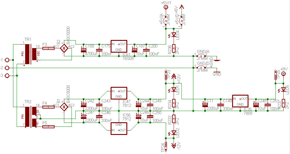
Hi everyone, today I did the first test-run of the power supply proposed in this topic. Based on this test-run I can confirm that the power supply is working perfectly! I did not yet have the chance to push it to its limits and see how it handles, but I can confirm a stable voltage on all outputs! This is the latest schematic: http://members.home.nl/r.j.vlek/psu2.jpg It can deliver at most (but that is if the transformers can supply it): +12V (1A) -12V (1A) +5V (2A) +9V (the maximum depends on the current drawn from the +12V. If the +12V is not used the +9V can deliver 1A maximum.). Note: X1 is a connector with 6 pins. Pin 1 and 2 are connected to a 1x9V transformer. Pin 3 is earth. Pin 4, 5 and 6 are connected to a 2x15V transformer where pin 5 is the center tapped one. Pin 1 and 4 should be in fase. In my design the PSU schematic is part of a big PCB with an 8xMBSID + 8xMoog filter. The transformers are on a seperate board because I did not want 230V on my main PCB. Anyone interested in more details: feel free to send me a private message. Kind regards, Rutger
-

PIC branden? Kan ik tegenwoordig voor je doen ;)
rutgerv replied to NorthernLightX's topic in Nederlands
Ik heb sinds het weekend ook een werkende PIC-brander waarmee ook de nieuwe PIC18F4685 te branden is (MB_SID V2), als ik iemand hier een dienst mee kan bewijzen hoor ik het wel :). Groeten, Rutger -
Hi Thorsten, thanks for the reply on the super-poly mode! I've just finished the design of one big PCB in Eagle and sent it to Gold Phoenix PCB for manufacturing. It contains: -8 SID's (jumpers to select the proper voltage and caps for different chips) -4 cores -the master core with 8 banksticks, display connections and step B surface -4 rows of AOUT_LC's (resulting in 12 CV outputs at 12-bit resolution) -8 independant Moog filters with CV controlled cutoff and resonance (!) (however to keep the number of AOUT_LC's down the filters share the resonance CV in pairs (no need for differences in resonance between left and right channel)) -Output stage/mixer and headphone amp -Custom PSU (+12V/-12V/+9V/+5VDigital/+5VAnalog seperate analog and digital grounds) When the hardware is finished I'll have to do some small modifications to get the AOUT_LC's set to the 12-bit resolution for every output (and not the 2*8 or 1*12/1*4). When I have it working I'll be happy to help out with experimenting and programming the superpoly mode! Greetings, Rutger
-
Nice work TK! what is the reason for the choice of a 6-note polyphonic mode? Why not 8? Is the PIC's processing power the limiting factor? The reason I ask is because I've almost finished the design of a single PCB containing 8xMBSid + 8xMoog filter and I was hoping to use this hardware for an 8-voice polyphonic synth (or a 4-voice stereo poly synth). I treat each SID as if it's a single voice with 3 OSC's. So each SID has an independant signal path, through a Moog filter to an output. Greetings, Rutger
-
I think a VCA would be nice to have in the feedback loop so you can make the amount of feedback voltage controllable and store this setting within a patch. However, stability might be an issue. A short delay might be interesting too by the way to create some weird flanging effects.
-
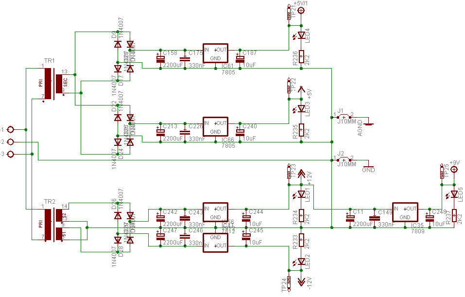
Thanks for the response, guys (and girls?)! I've worked on the schematic again. I still got the 9V regulator behind the 12V, but I've taken out the 2200uF cap and the 5V now comes from a single 78S05 (2 amps). I will be testing this powersupply within a couple of weeks and I'll let you know of it works! If it does and behaves as expected I'm willing to share the latest (known to work) schematic and possibly redesign the PSU to fit on a small single sided PCB. This will probably be a nice contribution to the people who want to build a big MBSID V2 and run into the limits of the C64 PSU. Greetings, Rutger
-
Important note about labling of MIDIbox SID V2 Frontpanel
rutgerv replied to TK.'s topic in MIDIbox SID
That's interesting news! Does it mean that the new step A surface will require an extra DIN and DOUT module? Greetings, Rutger -
Hi guys, to keep things going I've been working on a new design today. As Mike pointed out was an error in the connection of TR2, this is now corrected. I also replaced the diodes with a bridge rectifier B40C5000 (capable of 3.3A without heat sink). So, attached to this message a new design is added. I still do NOT have a solution for the grounding problem. I don't want to use multiple grounds at different potentials within the circuit, so i'm very open for suggestions to make this work with two transformers, one of which is center tapped. Greetings, Rutger p.s. Perhaps joining grounds would not be a problem if both transformers were center tapped?

-
Hi Altitude, thank you for the clear explanation in your updated post! I already had the feeling that this would become a problem...but what would the solution be? Is it impossible to use multiple transformers with a common ground? About the transformer for the 5V you advised to use a 6V/AC rated one...how about the 2x15V transformer? Is this overrated too? Greetings, Rutger
-
Hi, wow, these tips are of great value! Thank you very much. I've already modified the design of the 5V rails to use 1 bridge rectifier and I like the suggestion of the big 4700uF cap and the extra 100nF ceramics. I have considered the use of a single 7805S (2Amps), but I'm not sure if I can get rid of the heat properly...I'm afraid that regular heat sinks will not cool enough to get the 2Amps from it. Anyone experienced with the 7805S? Finally I'm open to suggestions about the ground-connections. My feeling tells me there's something wrong with it. Somehow I'm afraid that there will be a difference in potential between the ground that comes from the TR2 and the ground that comes from the TR1. Connecting them seems scary to me.... does someone know for sure how the grounds should be connected in the case of two transformers? Greetings, Rutger
-
Hi Flying Panther, thanks for the message! My main reason for this design was to keep down the heat and the physical size of the transformers and still deliver quite some current. At the moment I've estimated that my SID PCB will draw 1500mA on the 5V together, but I'd like to have some headroom so I'll put in a 1.8A transformer or something. Dividing the 5V lines over 2 regulators keeps down the heat on each of them and delivers a clean analog 5V line. On the +12 and -12 rail I estimated that the filters and headphone buffer use about 320mA. The SID's will draw either 320mA extra on the +12 rail or on the +9 rail (depending on a jumper setting near the SID socket). The 2x15V transformer gives about 1A at each rail, so that plenty of headroom. I'm planning to exchange the diodes with a B40C5000 rectifier and since it can handle up to 3.3A the 5V lines may share the same rectifier (to keep down the costs and number of components). I also plan to add fuses after each transformer to protect the transformers against overheating, melting, etc, instead of any trouble in the circuit. The powersupply will be added to 1 single PCB containing all components of my SID synth. One thing that i'm a little bit scared about is that I have to add a 230V connector and PCB traces to this PCB to connect the transformers. I'm not really happy about that....for safety reasons, but I have limited options in a 2HE rack space. Greetings, Rutger
-
---MODIFIED: A final working version of the PSU design can be found below!--- Hi everyone, I'm working on a rather big 8xSID module with 8 seperate Moog filters controlled by AOUT_LC modules. For this project the modified C64 power supply may not be powerfull enough, so I designed my own and I was hoping that some of you could double-check my design and tell me if everything is allright. The circuit is attached to this message as JPEG. Some comment with it: - To the left the 230V power input connector (pin2 is ground) - TR1 = Transformer(230V to 9V), TR2 = Transformer(230V to 2x15V) - The TR1 output drives 2 independant 5 volt regulation circuits, this is because I want to separate the digital and analog 5V lines as much as possible and I want to distribute the current load over two 7805 regulators (gets less hot than 1). - The TR2 output drives a +12V and -12V regulation circuit and the +12V output is fed into a +9V regulation circuit. This gives in total: +5V (= 5V line for digital stuff) +5V/1 (= 5V line for analog stuff) +9V (=for SID modules) +12V (=for SID modules and op-amps) -12V (=for op-amps) AGND (=ground for analog stuff) GND (=ground for digital stuff) I have two questions: 1. Is the wiring and circuit okay? 2. Is it alright two join all grounds at the power supply? I have joined the relative ground of all regulation circuits with each other and with the earth pin on the power inlet. Greetings, Rutger
-
Hi Wilba, thanx for the info! I still find it quite hard to make a good estimate of the required amount of Amps of the powersupply in my case. I've designed a PCB with: 8x SID 4x CORE (1 of them with LCD-connection) 2x DIN (for control surface) 8x 'bankstick' EEPROM 4x AOUT_LC (each has 4 x 74HC595) 8x Moog Ladder filter with added CV control for resonance 1x Mixer/Output stage/Headphone buffer I left out the power regulation circuitry for each module because I plan to create one powersupply that delivers all required voltages. These are the powerlines I used in the design: 5V - analog (SID's) 5V - digital (all digital stuff) 9V (SID's ....a jumper selects the proper voltage for the type of SID) 12V (SID's and all op-amps ....a jumper selects the proper voltage for the type of SID) -12V (op-amps) In my opinion there are two options for a global power supply: - One huge dual 12V transformer and regulators to deliver the 9V and 5V - One dual 12V transformer (the 9V will be downregulated) and one 5V regulator In both cases I'm wondering what the amount of Amps for the supply should be... Greetings, Rutger
-
Hi Wilba, just curious...what kind of powersupply do you use to run this 8xSID module on? Do you know anything about the powerconsumption of the board? The ucapps.de website used to say '1A PSU' for the MB_SID V1 with 4 SID's and control surface step C. Is this still valid for the new generation of 8xSID MidiBoxes? Greetings, Rutger
-
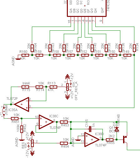
I've just made a new schematic that leaves out the TL072 and moves all trimming stuff to the first 1/4 TL074. Would this work?

-
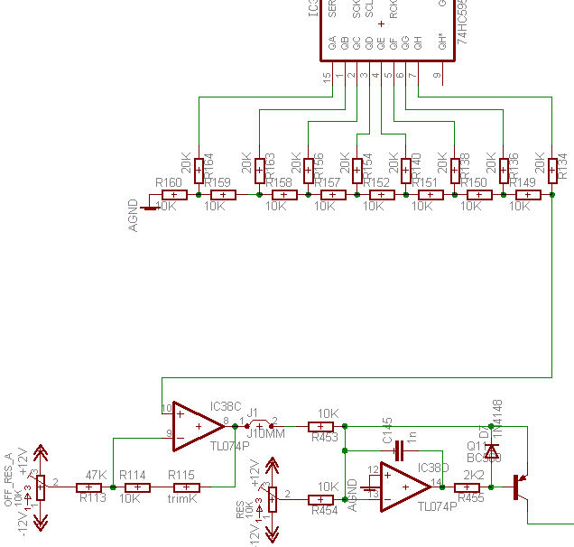
Ah I think I know understand what R451 and R452 are for. I guess this is a voltage divider that keeps the 10,67 specified voltage just below 10V at the input of the first 1/4 TL074. That raises another question: - Can I get rid of R451 and R452 if I calibrate the TL072 circuit to keep the voltage below 10V? I believe that should be possible.... In that case I could also take out the first 1/4 TL074 and use it in place of the TL072, right?
-
Hi everyone, as some of you already know I'm working on a 8xSID synth PCB and I'm hoping to include 8 Moog filters on it with CV control for Frequency and Resonance. One major issue in the whole process seems to be the maximum board size for a 19" module. To keep down the costs I want to design everything to fit on a single PCB that fits on the bottom of a 19" 1HE rack. I was hoping that someone could assist me in understanding the AOUT_LC module. I'm using an 8-bit configuration to control the Resonance. The attached file shows a part of the schematic. On the top the 74HC595. The output stage of the AOUT_LC is connected to the input stage of the resonance control. This uses half a TL074. The transistor on the bottom right of the schematic controls a LM13700 OTA. This OTA controls the amount of resonance. This is what I would like to know: 1) What is the voltage (max/11111111active and min/00000000) that comes out of the resistor network (i.e. pin 3 of the TL072 in the schematic). 2) How does R452 (tied to ground) affect the voltage going to the first 1/4 TL074? 2) Would it be possible to leave out the TL072 and use the 1/4 TL074 next in line to get the same kind of control over the range and the offset of the CV. What would happen with the resistor (R452) tied to ground? Greetings, Rutger

-
Hi Wilba, wow, i'm absolutely amazed by the job you've done routing everything manually in Protel! Even with the auto-router in Eagle I'm having a hard time getting boards of similar sizes and complexity routed. Maybe I just need a little more practice with Eagle. It doesn't have the best user interface i've seen (**huge understatement!**). Anyway...with some practice i'll get around it. Originally I started with a redesign of the Rick Jansen Moog filter. I've modified the resonance circuit to allow CV control and I was hoping that with SID V2 this filter could be integrated in the patch structure (i.e. no manual controls anymore over this filter!). But during this project my plans have extended somewhat: the new plan is to create an 8xMoog filter with CV controls for res and frq for each filter. This filter could be a nice addition to an 8xSID MidiBox with AOUT(_LC) modules. Sharing the shift registers is a very good idea! I didn't understand at first how the two SID's could operate independently, while sharing the shift registers, but now I do. If it's not too difficult to explain, would you mind sharing how exactly you modified this? Are all outputs of the shift registers (that are normally connected to one SID) simply attached to both SID's instead of one? Or does such a connection require extra components? I assume that also software adjustments are required...but actually I'm looking forward to do some modifications to learn how the MIOS system works. Greetings, Rutger
-
Hi Wilba! Nice work! I was wondering about the prototype PCB on the first page of this topic. How many layers did you use? Is it done with 2 layers (top, bottom?). Where did you fabricate it and what did it cost? I also noticed that you let both SID's on each core share the two multiplexers. Isn't this a limitation for more polyphony? I assume that both SID's always play the same patch... Another question I have is about PCB design in general. In most schematics each power pin of an IC has a decoupling capacitor next to it to prevent noise from a change in power consumption of the IC on the power rails. How important is it to have these capacitors close to the IC in the final PCB layout? The reason I ask, is because I have seen the inside of some commodores and on some MainBoards all decoupling capacitors seem to have been put together in a corner of the board. Doesn't this cancel the effect that these capacitors should have? Another thing I was wondering about, is how you wired the power rails on the prototype PCB. Did you somehow force a daisy chained connection to all modules on the board? Or did you simple let Eagle choose the best routing? Greetings, Rutger ps. I hope i'm not stealing your thunder, but I'm working on something similar. For my own use I want to make a 8x SID board with 4 cores (V2!). I would like to use the 8 SID's as a 4-voice polyphonic stereo synth or a 8-voice polyphonic (but mono) synth, or maybe even a multitimbral synth. Behind each SID i'm building a cheap version of the Rick Jansen Moog filter, controlled by AOUT_LC modules. I'm considering to modify the filter with some voltage controlled distortion and maybe a VCA after it (but this is a bit redundant since the SID's have their own VCA. The only reason for it is to shut-up the filter when it's self oscillating).