
latigid on
-
Posts
2,524 -
Joined
-
Last visited
-
Days Won
149
Content Type
Profiles
Forums
Blogs
Gallery
Posts posted by latigid on
-
-
Please explain your set up. Are you using the Wilba control surface? Do you have the SEQ running correctly? Have you edited the hardware config file?
-
No, what's your set up? Have you level-shifted the 3.3 V signal?
-
Just a thought here: J19 on the LPC core is already buffered, while on the STM 32 it isn't. This might make all the difference!
Also, the pinning seems to be a bit inconsistent:
J19:  Vs  Vd  So  Sc  Rc1
J1 :  Vs  Vd  So  Rc  Md
TK :  Vs  Vd  Rc1 So  Sc
The J19-J1 pinning is therefore not 1:1?
-
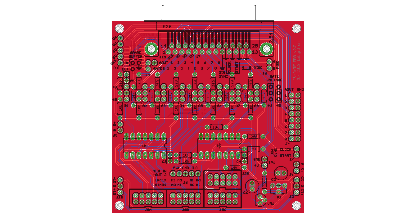
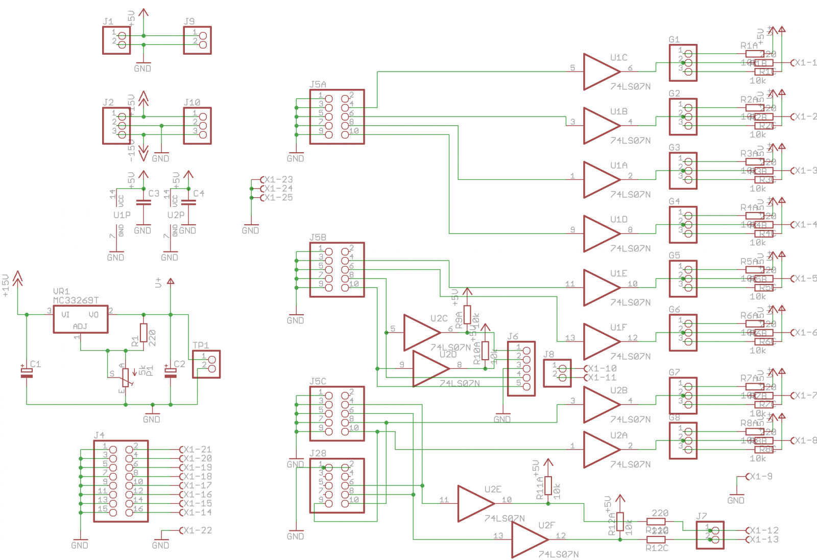
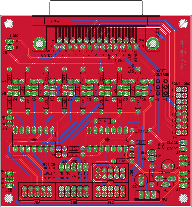
This revision has a connector for J19, for ocassions when the AOUT module is outside the case. The three data lines are buffered by a CD4050, unfortunately it's SMD as I couldn't find a part that would fit easily. One of the additional buffers is available, there wasn't room to route up the other two so they are tied to ground. The connectors share the same pins as J4 from the AOUT.
 EDIT: Pic
 -
It might help if you list your location. Are these the two-piece PCBs which need wiring together?
-
-
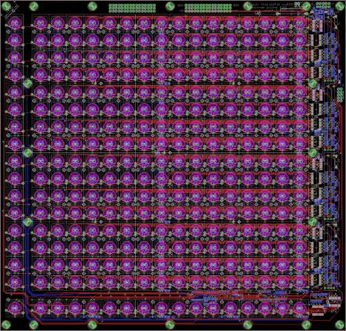
Maybe run the Eagle DRC? There are two vias which overlap and many traces below the minimum clearance. Best of luck!
-
Good job, but I don't think that there are enough mount holes. These things are pretty long, covered in components and one would be applying pressure over the whole surface. Too much flex in my opinion.
-
I can squeeze in one more connector on the top left side for people who will send the signals from J19 to an external AOUT module. Should the three data lines be buffered also? This should be doable with an SMT chip.
-
Okay, I think I'm done now.
I think that it looks okay but I'm not 100% sure on the regulator circuit. If somebody could check that would be great.
Also: no answer as of yet on the MIDI IN/OUT 3 situation. In any case, I have brought out the 3.3 V and 5.0 V connections.
-
It might involve specially programmed 16F88s. Note that the Quad IIC has a circuit-level implementation (EDIT pins 12 and 13 as shown on the schem.) for addressing the IICs (MIDI OUTs), so you might need a custom PCB for more outputs.
-
 1
1
-
-
USB MIDI perhaps?
-
I think that this can be more efficient with only two 7407 chips and a switchable pull-up voltage instead. Working on this now.
-
If you can't beat 'em, join 'em.
Following a discovery that the I am working on a revised design based on SN7407 level shifters.
(If you want a board from the the buffers work as expected, please PM me for details.)
Simple enough circuit but I have several questions.
First off: any problem with cascading the buffers this way? The idea is to have a switchable output between +5 (also serving as Vdd for the ICs) and an adjustable voltage which is derived from a low-dropout regulator (say 12 V or higher).
It is more simple to route when the output of the first buffer connects to the input of the second, but would it be better to tie the inputs of both buffers together instead?
What should the handling of MIDI IN 3 and MIDI OUT 3 be?
Presumably MIDI IN 3 should go through an optocoupler with a 3.3 V pull-up on the Core side:
http://ucapps.de/mbhp/mbhp_core_lpc17_midi3_midi4_extension.pdf
Hence, no level shifting is necessary I think.
But for MIDI OUT 3?
From the Quad-IIC schematic it is not clear whether the signal needs to be level-shifted. Will a 3.3 V output be compatible with the 8-bit core of the BLM?
In this case, MIDI OUT 3 is level shifted:
http://ucapps.de/mbhp/mbhp_core_lpc17_output_buffers.pdf
For these two, it isn't:
http://ucapps.de/mbhp/mbhp_core_stm32_midi3_extension.pdf
http://ucapps.de/midibox_blm/blm_connector_mbseq.pdf
There is a 3.3 V pull-up for the LPC core:
http://ucapps.de/mbhp/mbhp_core_lpc17_midi3_midi4_extension.pdf
Even though I will not use the LPC core, I plan to make it compatible with both for the greatest flexibility.
Some clarification would be welcome.
Cheers,
-
I'm not really familiar with the LTC module sorry, and I mis-spoke when I said MIDI thru before, of course you would be just duplicating the ports.
It seems as if the serial functionality of the LTC module is not really useful any more. As far as I know you can use the buffer/level shifter IC to do this duplication.
Hope that helps,
-
This is effectively like a MIDI thru port; using the IIC modules will give you the benefits of more channels, less configuration required, lower latency etc.
How many do you require? Are you aware of the Quad-IIC board available at SmashTV's shop?
-
No worries, it's outmoded hardware anyway :tongue:
Hopefully I can come up with something to work with my board layout.
-
Thanks TK, but I seem to be getting conflicting advice. What does the setting "J5_ENABLED 2" actually do then?
-
I have 10k resistor networks connected to each gate and DIN sync, and the common pin is showing +5V.
In the HW file I haveJ5_ENABLED 2
But I only see around 3.7 V for each gate.
Any suggestions?
-
Glad that you're okay! It's hard to imagine so much damage being done in so little time...
Wishing you the best,
Andy
-
I think that we're over the 8 boards that I have available, but there's always the possibility that people back out etc. I am currently waiting on a bit of advice with regard to level-shifting the gates from the STM32 core, I'd rather not fry my pins :)I'm happy to organise another run if there is demand for one.
-
My plan, unless anybody tells me otherwise (please do if this sounds stupid) is to solder 220 ohm resistor arrays to the core32 pcb in order to achieve the +5 V signals.
Will this work with all outputs, including the 8 gates, MIDI I/O 3 and DIN sync start/clock? Or do these pins also require setting to open drain mode?
Thanks,
EDIT: or is 1k or 10k more appropriate? There is a +5 V rail running very close to J5A/B/C
-
And dare I ask, in what situations would one use open drain mode?
-
Just because I have things soldered already :smile:
I was hoping for switchable gain between +5 V and something arbitrary like +12 V, but like you say I can just fiddle with the feedback resistors to tailor the gain level.
Many thanks and greetings,
Andy
Edit: the gates should be enabled, but not in open drain mode, correct?J5_ENABLED 1
MIDI Box CV dead gates?
in Testing/Troubleshooting
Posted
Protection: yes, definitely. The two systems used are buffers/level shifters (also gives you a +5 V logic level in the case of newer Core modules) and 220R resistors for short circuit protection.