
latigid on
-
Posts
2,524 -
Joined
-
Last visited
-
Days Won
149
Content Type
Profiles
Forums
Blogs
Gallery
Posts posted by latigid on
-
-
sneakthief, I see some issues with one standard of input: If a bipolar CV (like an LFO) is plugged in, the negative portion of the waveform will be clipped to ~0 V by the Schottky diode. Also for nominal signals of say 0-5 V you lose half the ADC resolution as the full scale input is 10 V. But the option should be there to choose your own pre-ADC treatment. I will get around to a board layout at some point, just a bit busy at the moment.
-
Wow, looks awesome!
So, now we have a gate to MIDI converter -- any thoughts on CV-MIDI conversion at 1 V/octave?
With the AIN scaling/protection circuits it seems to be difficult to decide on one standard, so I propose on a final panel a mixture of 0-5, 0-10 and -5 to +5 inputs, hopefully that's workable with the correct offsets. Alternatively each input could have an attenuator:
-
You might've fried your LCD, that's easy to do. You describe shorting the backlight, well if you've applied a high current across any of the data lines that could knock out some of the circuitry. Do you have the option of using a second backlight for a test? If so, be sure you don't have any shorts that might repeat the process and outcome.
-
With the discussion on the CV V2 topic
I'm thinking about what this means for the SEQ application. I would like to have both in a modular set up: MBSEQ for, well, sequences, and MBCV for interesting envelopes, LFOs, bussed knob controllers, scopes etc.
There's a bit of overlap: the SEQ sends out 8 channels of CV/Gate and DIN SYNC while the MBCV can additionally output more clock signals and receive analogue inputs and a clock as control sources.
The use of balanced line drivers will be useful for both boxes for AOUT, but how about the digital signals?
The hardware config file for the SEQ lists SR outputs for gates, so is there a possibility of avoiding J5A/B etc. and just sending the balanced DOUT SRIO chain instead?
And what about LED indication for the gates? Could a different SR output a 5 V signal to turn a gate on and off? Reading the config file maybe this is not possible, what is the explanation? The parts count would be a bit lower than using common emitter LED drivers.
-
-
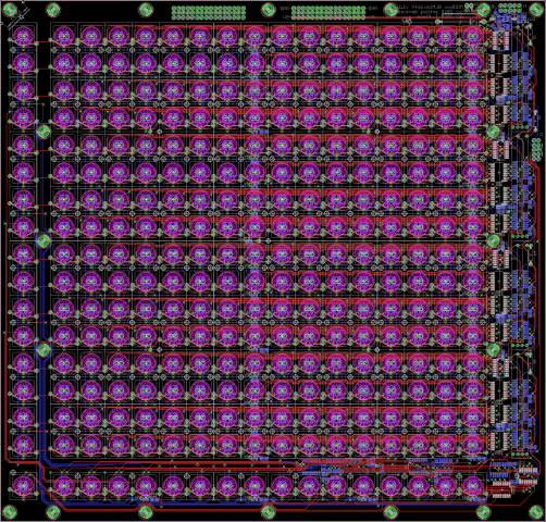
Hmm, I had a try at putting 32 sockets on a 4.05" board (basically the max. height for a Eurorack PCB):
8 gate
8 CV
8 AIN
7 Clock
1 Sync in
and it's pretty tight even at 2.2" (for a 12 HP panel), especially with another multipin connector and mounting holes.
I suggest a DB-25 (or whatever connector) is mounted on a PCB with all of the interfacing circuitry (line receivers, analogue input protection circuits, pass-through for AOUT and DOUT). All of the other sockets could be panel mounted and wired to MTA 100-style connectors or similar.
I know the trend is towards super shallow modules with no panel wiring but this would give a better return on investment for PCB space. Also it is customisable and more flexible for other modular formats (5U, Serge etc.) or even standalone MBCV enclosures.
-
Quick and naive question: are the serial clocks independent; could they be shared too?
-
I was considering a dual use board, one for MBseq and one for MBCV. This is for us old farts who are still on STM32F1 cores!
So we could get away with a 15 pin connector for the digital serial signals and a 9 pin for AINs.
-
Great job TK!
What about this for the cable pinning?:
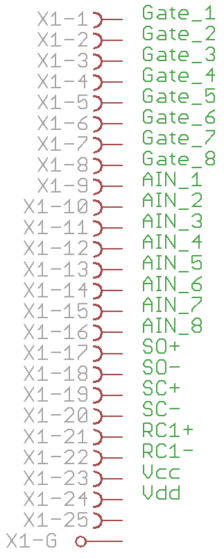
Unfortunately this leaves no room for clock signals (DIN sync/start). Shall we move to a larger cable like DC-37?
http://en.wikipedia.org/wiki/D-subminiature
Otherwise a higher density version might be an option, the problem then becomes finding a source for the more esoteric connectors...
-
Yep, a fair amount of work...
-
Hey,
They also sell capacitive TS overlays, just check through the menu on the left hand side. As far as I know these will also work with multi-touch gestures. As the interface is USB I guess all of the scanning hardware is compacted into the frame. Best of luck and let us know how you go!
Many Greets,
Andy
Ah, maybe they're infrared?? -
I was thinking of a non-tablet solution for a MIDIbox touchpad and came across these:
http://www.cyclotouch.com.au/product_info.php?products_id=2468
(you can also check out the other kits).
My thought was to design a 16x16+1 LED array PCB, then overlay a transparent panel with the touch matrix interfacing to a Core module running the BLM code. In the end, a commercial tablet already has an integrated processor, WiFi and a long-life battery for wireless connectivity.
-
New topic:
How about skipping ethernet altogether and going directly to WiFi? Adafruit offer a cheap breakout module running over SPI:
http://www.adafruit.com/products/1469
Is there a free SPI buss for this purpose? I notice the STM32F4 board does not yet have an ethernet connector.
-
Transfering the serial signals to an external breakout board is problematic, because actually the cable to an AOUT module shouldn't be longer than 30 cm!
We have to do some experiments with line drivers and receivers, see also the bottom of this posting:
Best Regards, Thorsten.
Even when that signal is buffered? JBdiver reports successful signal transfer to his breakout module using only the 541 buffer of LPC17
-
I'm assuming most people would prefer to have the jacks in an accessible place, meaning you could mount the CV/gate jacks in a Eurorack panel and power it with a modular's +/-12V. Or in a little box like TK does.
What about using a 15-pin VGA D-SUB connector between the CS and the outputs? It has 15 pins plus shield:
- 8 pins for gate
- 1 pin for clock
- 1 pin for start/stop
- 5 pins for AOUT (Vs, Vd, CS, S1, SC)
- 1 pin for the shielding ground
Someone would of course have to test this first to make sure there isn't too much interference from the digital signals. Maybe a 1m cable VGA would suffice?
To conclude, the Eurorack panel would have a 15-pin VGA D-SUB connector, 8 CV out jacks, 8 gate out jacks, 1 clock jack, 1 start-stop jack.
You could optionally add 8 buffered LED's for the gates.
Let's just think about this a bit more:
8 gates, but up to 64 with DOUT/DIO_MATRIX.
DIN SYNC is 1 start/stop but up to 7 clock divisions/multiples.
AOUT is really 6 signals (Vs, Vd, SO(SI), SC, RC1 and RC2) but Vs is common to the Core and doesn't need a separate ground.
1 sync input to control the master clock/ forwarded to the additional clock outs.
What about analogue inputs? These would be pretty cool to interface from a modular system back to the Core. Diode clamps to protect the input pins?
We're getting into quite a few signal lines now, too many for a DB-15!
But for a basic usecase:
8 gates
5 AOUT
1 clock start
7 clock out
1 sync in
8 AIN
1 signal ground
31 pins ---> DB-36/Centronics?
With only one clock out you'd be back to DB-25.
-
Okay, it makes sense for all the gates to be on J5A/J5B (different to the other Cores). Right, I see the MIDI IO on J11E.
For MBCV V2 I guess J5A/B will be used as analogue inputs then?
>>> Maybe I will create a board for STM32F1 and LPC17 and we can sort out another one later for F4.
Best regards,
Andy
-
TK, do you have thoughts on pinouts for the "J5C" connector on STM32F4? I will put together a DB-15 breakout/level shifter board for Gates 1-8, DIN Start and Clock, and MIDI OUT 3 (no room on the DB-15).
Will it be more like STM32F1 or LPC17?
Thanks,
Andy
-
The back of the board is a better place to put them, although you only really need a header for J1 (/J2), the rest could be wired directly. Try sliding off the plastic base (or cutting it) and push each pin out individually. Divide and conquer is the motto for multi-pin desoldering.
-
Getting closer:
Data lines are okay?
-
The J1/J2 sockets are not "polarized" (no notch) - probably you decided this due to the missing space.
But I would prefer this against J2 - so, just remove J2 again to make place for a polarized J1 connector.
If somebody would like to chain multiple modules, he has to build an external adapter and solder it directly on the required pins.
Okay, I will not use my version in this way as the connections will be "sammich" style to another board. But I agree, polarised connectors make good sense. Unfortunately that makes the board bigger, but I needed to give proper clearance to the mounting holes anyway. So I moved the trimmers around and that leaves room for another connector: J2 for serial output. Can I please check pins with you because the AOUT_NG does not seem to match 1:1 with the newer Cores' J19?
AOUT    : Vs Vd CS SI SC
AOUT_LC : Vs Vd SO SC RC
AOUT_NG : Vs Vd SO RC MD (?, from wiki picture)
        : Vs Vd FS DIN SCLK (connections to DAC on schematic)

AINSER64: Vs Vd DI SC RC1
          Vs Vd DO SC RC2
           _____| |_____

CORE(32): Vs Vd SO SC RC1
          Vs Vd SI SC RC2
           _____| |_____
So, are these connections correct ?
CORE(32):
Vs Vd SO SC RC1
Vs Vd SI SC RC2
______| |______

AOUT_EURO J1:
Vs Vd DIN SCLK RC1   J3 chip select
Vs Vd nc  SCLK RC2    RC1/RC2 => FS
______| |______

AOUT_EURO J2:
Vs Vd DOUT SCLK RC1
Vs Vd nc   SCLK RC2
______| |______
to which ground are they connected?I would use the digital GND for both planes.
Best Regards, Thorsten.
Sorry for the confusion, there is essentially one ground (both top and bottom layers) but GND and AGND are connected only at one point on the board. There is a "bridge" for Vd and Vref to travel on. My question was: should this bridge be on both top and bottom layers?
Thanks! I'll keep chipping away at it.
-
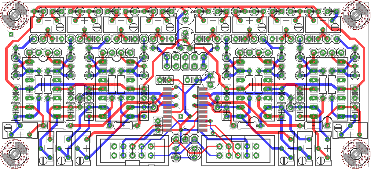
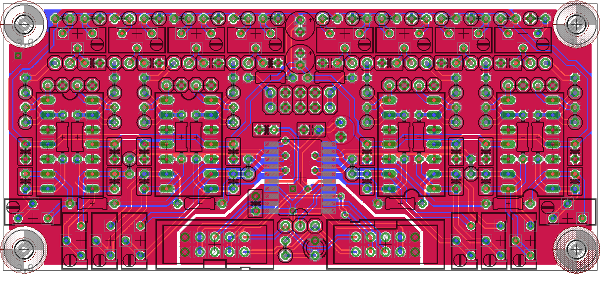
PCB layouts without and with GND plane:
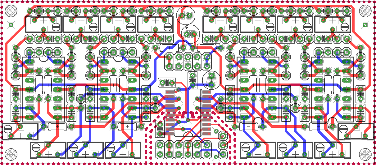
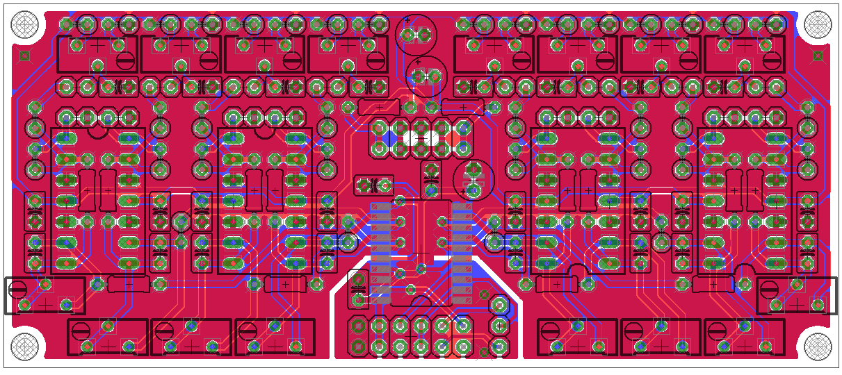
Routing was a bit tight for this format, but I think it works okay.
I added a chip select line and put the DOUT signal on the same connector. Hopefully this is okay if somebody wants to chain more than one module.
I isolated AGND and GND, and both top and bottom planes are connected. Is this a good idea? On the AOUT_NG PCB only the top layer is connected.
-
Yes, I've made one
-
Très cool! Tu as utilisé un Core 8 ou 32 bit?
-
Routing everything now, a good holiday project!
Question: will any application make use of J2 (serial out) for chaining multiple modules? It seems unlikely so I would prefer to remove this connector. In this case, would it be better to terminate the digital out in some way (tied high or low)?
MB-LRE8x2CS rev 4.6 BULK ORDER spring 2014
in Bulk Orders
Posted
Nice, have improvements been made with regard to LED saturation?