Leaderboard


Popular Content
Showing content with the highest reputation on 12/14/2017 in all areas
-
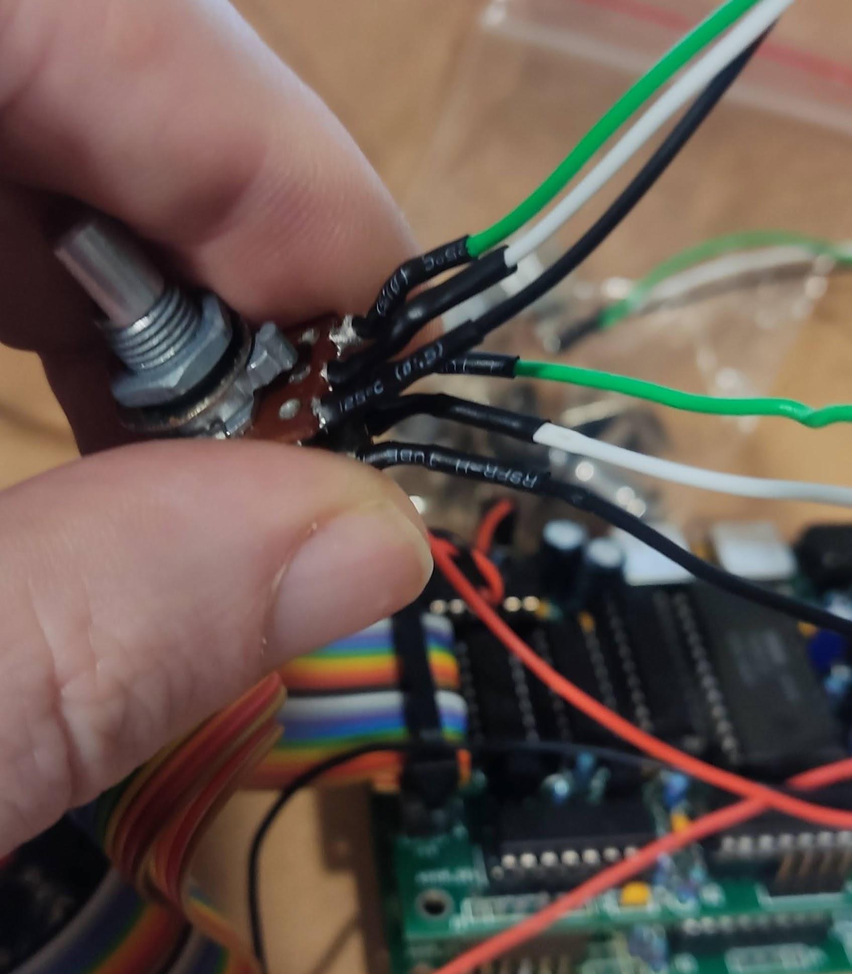
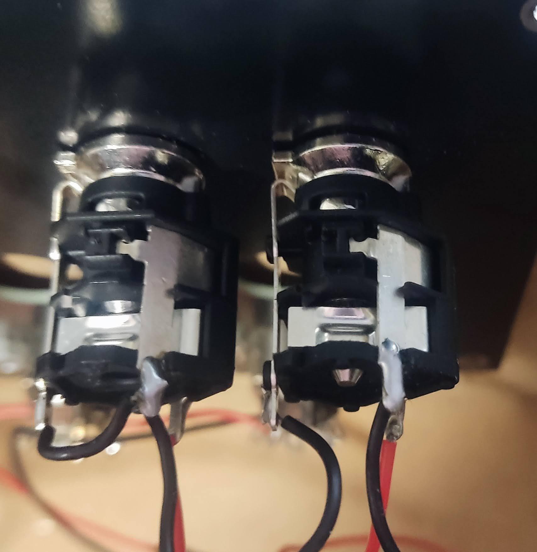
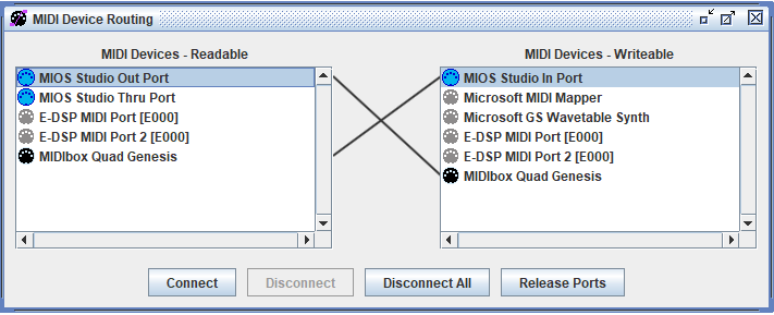
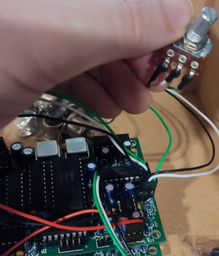
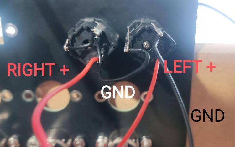
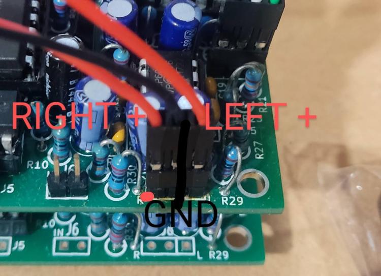
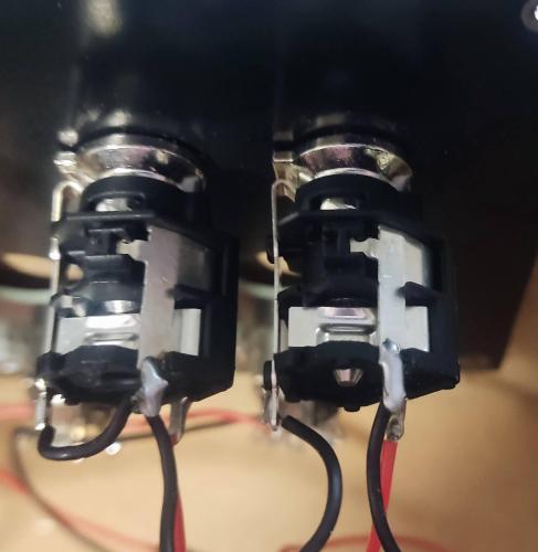
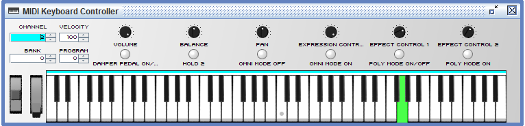
Step 12: Testing the sound To test the sound we need to either connect the potentiometers to R18, R19, and R20 headers of the Genesis Module, or we can connect jumper wires to the Input and Output pins of each header to test it more quickly. If you want to connect the potentiometers and L/R audio sockets scroll down further. Jumper the following points on R18,R19 and R20: As you can see the Square pads are GND, the next is Input and the 3rd Pad is Output. Crimp a 3 pin audio cable for the Stereo Output header J8, and solder the audio jacks according to the folliwing pinout: Pin Label Function 1 – Left channel output 2 GND Ground 3 – Right channel output In the picture below I just used a crocodile clip attached to the Tip of a 3.5mm audio cable as I'm waiting on a delivery of audio jacks. OR Solder the potentiometers and audio sockets. First we will solder and crimp the wires for the YM2612 output. Crimp R19 wires to fit a 3 pin Dupont connector that goes into the R19 pins of the Genesis Module. Then solder the other end of the wires the bottom terminals of the dual gang pot. Black =GND White = Input Green = Output Crimp R18 wires to fit a 3 pin Dupont Connector that goes to the R18 pins of the Genesis Module. Then solder the other end of the wires to the top terminals of the dual gang pot. Next we will cirmp solder the wires for the PSG which uses the Single Gang Potentiometer. Crimp 3 wires for the 3 pin Dupont Connector which goes to the R20 pins on the Genesis Module. From Left to Right: Black = GND White = Input Green = Output Now we will crimp and solder 3 wires to the 1/4" audio sockets. Crimp 3 wires and use a 3 pin dupont connector as shown.. Ensure the 1/4" audio jacks are mounted so that the correctly so that the metal contacts are on top as shown in this picture: Solder the LEFT+ (positive) wire to the bottom right of the terminal of the L/Mono audio socket as shown. Solder the GND wire tom the top right terminal of the Left/ Mono audio socket as shown. Solder the RIGHT+ (positive) wire to the bottom right terminal of the Right audio socket as shown. Then solder a short GND wire from the leftmost terminal of the L/Mono socketr to the Top right terminal of the Right socket. I also soldered another short GND wire from the Top Right terminal of the Right Audio Socket to the leftmost terminal of the Right Socket. Plug in your 1/4" cables to the Left and Right audio sockets to test the audio in the next step. Next ensure the Java runtime is installed on your computer, if it isn't then install the latest runtime from www.java.com Download and extract MIOS Studio 1 from this link, but do not run yet! http://www.midibox.org/miosstudio/MIOSStudio_beta9_4.zip (We are using the older version of MIOS because it allows us to right click the keyboard and hold notes to test polyphony easier using just a mouse.) Power on your MIDIbox Quad Genesis and connect it to your PC/Mac via the Micro USB Cable. Wait for the LCD Screen to show the status screen and now run the MIOS Studio 1 .jar file. Click Options -> MIDI Device Routing and Connect MIOS Studio Out to MIDIbox Quad Genesis on the right hand side, and connect MIOS Studio In Port to MIDIbox QUad Genesis on the Left hand side, as shown in this picture: Close the window, and change the MIDI Channel to Channel 2 on the Virtual MIDI Keyboard Controller: Now play a note and you should hear a piano patch play on the FM Chip! To test the polyphony right click on 4 notes and each note play. Clear the 4 notes by left clicking on them (If you right click on more than 4 notes, youll notice some notes will no longer play - this is because in its current state MIDIbox quad genesis is expecting 4 FM chips which are not there, and is trying to allocate notes to the 2nd, 3rd and 4th chip!) Now set the MIDI channel to channel 3 and play a note to test the PSG Chip. Right click on 4 notes and ensure they play. If everything is setup properly you should have sound!
.thumb.jpg.5f46516a296618d5936bb4b6d38a4f49.jpg)

.thumb.jpg.d18864699678b6e4163d5aa555327f2a.jpg)

 1 point
 -
//write u8 PB8[STEP_NUM*2]; for (i=0; i<STEP_NUM; i++){ PB8[i*2] = (u8)(PB[track][i] & 0xff); PB8[i*2+1] = (u8)(PB[track][i] >> 8); } FILE_WriteBuffer((u8 *)PB8 , sizeof(PB8)); //read u8 PB8[STEP_NUM*2]; FILE_ReadBuffer((u8 *)PB8 , sizeof(PB8)); for (i=0; i<STEP_NUM; i++){ PB[track][i] = (u16)((PB8[i*2+1] << 8) + PB8[i*2]); } much less beautiful1 point
-
Try: // write FILE_WriteBuffer((u8 *)PB[track], sizeof(PB[track]); // read FILE_ReadBuffer((u8 *)PB[track], sizeof(PB[track]); I did it and your project was compiled without error...1 point
-
What is the calling procedure? can you send me (PM) the project? I need a bigger view. I think structure can resolve write and read but I need to know how it is called. I'm not at home, nothing to do in the night in my hotel room, I can write something even if I haven't got any hardware to test it... Best1 point
.jpg.2c19904b6578d11d82111c21cd9844e1.jpg)
.jpg.e89bf382211f823cf022b2301ada6495.jpg)