
latigid on
-
Posts
2,524 -
Joined
-
Last visited
-
Days Won
149
Content Type
Profiles
Forums
Blogs
Gallery
Posts posted by latigid on
-
-
I can't quite picture the concept, could you draw something?
-
7 minutes ago, TheMentat said:
I've resolved the SW10 issue... bad solder joint on the super flux CC after I pulled the switch.
Good!
7 minutes ago, TheMentat said:While waiting for the new transistors, I swapped T15 and T16. Doing so switched the affected superfluxes to green (instead of red). This suggests a bad transistor which will also have to be replaced. I suspect I messed up some of these by eagerly trimming the RJ resistor legs.
Good to know. Depending on the reflow temperature, the component might also be damaged that way.
7 minutes ago, TheMentat said:Moving along, I've started mocking up the final assembly. For some reason, plugging in the displays will not allow the SEQ to boot (the green LED on the SDcard module does not light). This only occurs when I jumper J15_S. I suspect a short somewhere on the power rail for the displays... sound right?
Always check for shorts! On experience this is typically caused by a bad cable or excess copper on the connector end shorting on the OLED PCB. Depending on when your parcel arrived Peter might have put a piece of kapton tape on the OLED. You can try with a piece of paper or tape.
Also check R33D on the Core is 560R.
-
9 hours ago, TheMentat said:
- superflux 4,8,12 & 16 , and have a very slight red glow to them (like a short somewhere), and 20 & 24 also glow dimly...
I would suspect IC4 pin 1, R15, T15, RJ7, perhaps also IC4 pin 15, R16, T16, RJ8.
Also check the transistors on the rear of the board and their associated Schottky diodes.
9 hours ago, TheMentat said:- SW10 no longer illuminates the corresponding superflux (in fact, it slightly green illuminates the superflux on #2 above it)
Do you still get a DIN event in MIOS Studio?
Is the switch soldered in properly? The associated diode? If the other switches in the column work, then the matrix is okay and the issue might be with the LED itself or the switch of course.
-
Check T14 and R14!
Do you measure any voltage out of pin 2/R14? Follow that down to T14. When you read the T14 label right way up, you should have continuity to R14 on the top-right pin, +5V on the top left pin. The bottom pin is the source current for your green LEDs on columns 3/7.
-
Check the green diode functions by using a multimeter in diode mode (black probe to CC pin) directly on the LED legs.
Some of the soldering doesn't look like proper joints were made, so make sure to reflow the pins. It would be odd, but maybe on RJ3 and RJ7?
The description of the error points more to an issue with IC4 pin 2, R14 (resistor legs too long?), but from your picture these look okay. It might also be T14 on the front side of the board. This part of the schematic is on page 2.
-
Next steps would be to ask again whether you get any voltage out of the superDAC board channel 8 and then to measure voltages on the components/pins I mentioned. Perhaps take some better photos and lay the voltage measurements on top.
-
Any luck on reflowing the components I mentioned? From the behaviour I would guess 8R49 or R57 are not properly soldered.
-
8R49 looks like a cold-solder joint.
-
Cool, getting closer then!
The components to check on transmute8 are probably related to the second inverting stage, so pins 5,6,7 of IC4, 8R33 (maybe), 8R41, 8R49, C29 and R57.
Check if any of these parts are connected to 0V (ground). Only pin 5 of IC4 should be.
Do you measure voltage on R57?
Best,
Andy -
Hello,
2 hours ago, niles said:On the Midi IN4 and OUT4, I know they are planned for controlling the BLM at some point in the future, but in the meantime should they work as regular Midi in/out ports? I have a keystep plugged in and it works on IN1, IN2, and IN3, but not 4 (when viewing via midi monitor). Was curious if it's a midiseq software setting or intentionally hardwired to be different.
My vote goes to bad wiring on my part, but just double checking.
Thanks
IN4 will fit a DIN5 as well as a DIN8, but the pads are not connected to avoid potential conflicts when using a BLM and questions of "where's my 5th MIDI in??" If you want to do it anyway, you can add solder bridges here:
 2 hours ago, niles said:
EDIT - Actually the more I read on the USB OTG it seems like I should be able to plug the keystep into USB with the switch in the OTG position. Quick power cycle but still no activity on the midi monitor. The same if I try with my Novation SL MK2 midi keyboard. Both they keystep and SL are being powered by a PSU and not reliant on USB power. Do you need a special OTG cable for it to work?
Shouldn't need a special cable, but to be honest I've not played around much with the OTG stuff. Did you route the MIDI anywhere, set the channels up etc.?
-
For testing tranmute8, you can start with no other boards connected. Verify no shorts on the power rail, though if your rack powered up that's likely not an issue. After connecting the Eurorack power cable, you should measure +12V/-12V on pins 4/11 of the op amps. Check that the op amp orientation is correct with pin 1 near the IC1/2/3/4 label. C3/4 seem to be correct.
I think you should still get some output even with nothing connected to the op amp inputs. Outputs on J3 should each be at -5V.
You can verify your octal board with a working binaire board.
-
I think you need to test piece by piece.
First disconnect everything.
The ribbon cables should have the IDCs mounted with the notches/nubs oriented the same way relative to the cable (e.g. both pointing down along the cable).
http://ucapps.de/mbhp/mbhp_aout.pdf shows the connections of the DAC. For the midiphy superDAC, we use the modern pinout, so CS = RC1 on pin 10, SI = SO on pin 6 and SC is on pins 7/8.
Before powering up, ensure +5V is not shorted to 0V (ground). Check polarised components are properly oriented (seems good from the photo).
Connect a known good cable to J19s. Not J19A!
You should measure +5V on pins 3/4 of the IDC pin header and on pins 7/14/20 of the 525/5500.
After initialising in the SEQ, you should be able to measure voltage on the J1 pin header outputs: 0V at min setting and 2.048V at max setting. Out 1 is on the right by the J1 label, then going left, outs 2/3/4, 0V, no connection, 0V, then 5/6/7/8.
-
I'm not sure if you initiated the DAC. If you choose a track on the AOUT port but no module is configured, you won't get any change. The menu page I'm talking about is here:
 CV Configuration Page

This page allows to select the AOUT/AOUT_LC/AOUT_NG interface, to configure CV channel and gate parameters, and to configure the DIN Sync Clock output.
- CV: selects the CV channel (1..8)
- Curve: selects the output curve: V/Oct, Hz/V, Inverted
- SlewR(ate): allows to configure a slew rate (slack) in the range of 0..255 mS
- SusK: activates the "SusKey" function (also known as "fingered portamento"): the slew rate will only be activated if at least two notes are played. This allows to use the glide function to enable slew only on demand.
- PRng: sets the pitch range for pitch bender events (normally 2, use 12 or 24 to sweep over one, resp. two octaves)
- Gate: sets the gate polarity (positive or negative)
- Calibr.: allows to force different output voltages for calibration (Min/Middle/Max/1V, 2V, 4V, 8V)
- Clk: selects 1 of 8 clock outputs (available at a dedicated DOUT shift registered which has been configured with the CLK_SR parameter in the MBSEQ_HW.V4 file). Each clock has an individual clock divider, or can optionally be used to output a Start/Stop signal
- Rate: defines the output rate of the selected clock output (1, 2, 3, 4, 6, 8, 12, 16, 24, 32, 48, 96, 192, 384 ppqn and Start/Stop)
- Width: sets the pulsewidth of the clock output signal (1..255 mS)
- Module: selects the AOUT module which is connected to J19 of the core module (AOUT, AOUT_LC or AOUT_NG)
Did you reach this page and set the Module type to "AOUT"?
Thereafter you should be able to "Calibr[ate]" volts in steps from 1-10V and min/mid/max. This is also how you can fine-calibrate the channels.
Best,
Andy -
MAX525 should work too. You should be able to control/calibrate the AOUT channels from the config page. What AOUT config are you using?
The LEDs will indicate the approximate voltage, but will only be off at around 0V as there is an offset present.
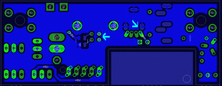
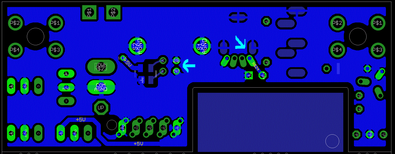
Photos of the boards so I can check if anything looks off? RC jumpers on the superDAC PCB not connected maybe? Correctly assembled cable attached to J19s?
-
I'm glad it was an easy fix!
For setting up the analogue channels, press Exit until you get to a list of menus then scroll through them with the datawheel until you get to CV configuration. The module type should be AOUT (probably AOUT_NG for non-midiphy boards). Changing the module type will always reset the data; useful if it gets corrupted and no power cycle is required.
The CV menu is where the outputs are calibrated and the clocks are configured.
For setting up the DOUT chain, count the number of 595 shift registers:
JA 1,2
lemec_L 3,4
lemec_R 5,6,7; 8,9so the first gates/clocks module will be at SR 10. Probably we should push the git update for a properly configured HWCFG file.
# CV and Gate/Trigger/Sync Setup
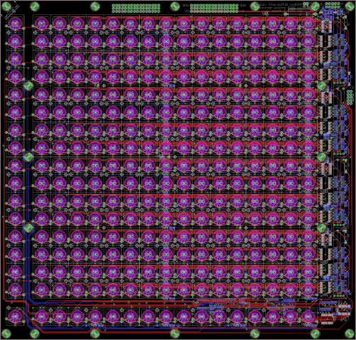
################################################## # CV and Gate/Trigger/Sync Setup ################################################## # AOUT interface now selected in CV Configuration Menu and stored in MBSEQ_GC.V4 file # please scroll through the menu to find this page! # the 8 CV gates can be assigned to a shift register (0=off, 1-32: number of shift register): # - 1st CV Gate available at DOUT SR output D7 # - 2nd CV Gate available at DOUT SR output D6 # - 3rd CV Gate available at DOUT SR output D5 # - ... # - 8th CV Gate available at DOUT SR output D0 CV_GATE_SR1 10 # and DIN Clock Outputs can be assigned to a shift register as well (0=off, 1-32: number of shift register): # D7..D0 will output individual clock or start/stop signals which can be configured in the CV configuration page CLK_SR 11 # additional gate triggers are available on common digital output pins of the # DOUT shift register chain - they are assigned to AOUT channel #16 (Note C-1, C#1, D-1, ...) # define the shift registers which should be used here (each provides 8 gates) # Note that SRs assigned to this function cannot be used as LED outputs (exclusive function) # Allowed values: 1-32, 0 disables the function, all other values invalid and not allowed DOUT_GATE_SR1 12 DOUT_GATE_SR2 0 DOUT_GATE_SR3 0 DOUT_GATE_SR4 0 DOUT_GATE_SR5 0 DOUT_GATE_SR6 0 DOUT_GATE_SR7 0 DOUT_GATE_SR8 0 # if set to 1, the additional DOUT "gates" will send 1mS pulses # useful for analog drums DOUT_1MS_TRIGGER 1 # should J5A/B/C outputs be enabled (0: no, 1: yes, 2: yes, but in open drain mode)? # - the 6 first AOUT gates will be forwarded to J5A/B # - the remaining last 2 AOUT gates are available at J5C.A10 and J5C.A11 (LPC17: J28.WS and J28.MCLK) # - DIN sync clock will be forwarded to J5C:A0 (LPC17: J28.SDA) # - DIN sync start/stop will be forwarded to J5C:A1 (LPC17: J28.SC) # - if open drain mode enabled (option 2), external pull-ups have to be connected to J5 pins # (advantage: pin levels can be pulled to 5V) # # NEVER USE THIS TOGETHER WITH ANALOG POTS - IT WILL CAUSE A SHORT CIRCUIT! J5_ENABLED 0 -
Directly connected means no line transmit board? How long is the cable?
What happens when you unplug J8/9 from le mec_R?
Are any ribbon cables improperly assembled (shorts etc.)?
Can you exit this menu?
Do you notice strange DIN events with MB_NG loaded?
-
The clock pulse can be varied in ms steps, but the triggers are either gate or 1ms. Does it work to use "gates" instead? Often a trigger input will react on the rising edge. If it's the falling edge though, then a gate wouldn't help.
I had a quick look through the code, but I couldn't find an obvious solution. Clocks are different to triggers, as the timing is always consistent relative to the master tempo.
-
Thanks for the info!
-
 1
1
-
-
Hello,
There is no power switch, as you should typically ensure a stable power rail before connecting data and the solution to that was a bit to complicated. Imagine if it was already connected to your computer with data being sent but no power rail because it was switched off. I'm honestly not sure if this would be a problem for the SEQ or the computer.
But if you would like to try, maybe something like this? You would need a USBA-USBA cable.
https://solarbotics.com/product/19068/
Or a USB B with a switch on it:
https://www.amazon.co.uk/Snowball-B-Male-Switch-Printers-devices/dp/B07GGT9XGT
If you would like to drill a hole in the case, how about interrupting the +5V line from the USB board to the Core? This assumes that you haven't used the Molex power headers on the USB board. Simply wire an SPST switch to reconnect the +5V.
-
Ha, you're right, the +5V plane is connected on this revision. Don't worry, we'll sort you out with a replacement. Peter will be in touch.
-
Please check the locations I mentioned and post a photo of your soldering.
Don't worry, the pours are not connected otherwise nobody's board would work...
-
Can you post a picture of the soldering? The most likely place is on either of the two USB connectors. This is the bottom of the board with the +5V and 0V connections highlighted.
-
RME Fireface should work.
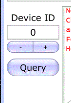
You can also change IDs through MIDI:
Quotechange_id_v1_9g.zip This program allows you to change the ID header without reburning the chip --- use this program with care and read the informations given in README.txt! I'm not sure if it's possible to change IDs if they're all connected in the MB-6582 with the same ID. If it doesn't work, consider removing all but one PIC when changing.
How is J11 set?
QuoteWhat is the function of J11 (directly below U1_Core1)?
J11 (not J11_CORE1) is a 4×2 pin header which controls which Core (PIC Tx pin) is connected to the MIDI Out port. You would only need to use this once for the first upload of MIOS and the MB-SID V2 firmware, thereafter connect the master PIC (1) to the MIDI out and after uploading new MB-SID V2 firmware, the master PIC can clone itself to the other PICs across the CAN bus. NOTE: All Cores (PIC Rx pin) are connected to the MIDI In port. The different device ID (0,1,2,3) on each PIC determines which PIC receives an upload, J11 is used to get “feedback” from that PIC during the upload
Select the ID in MIOS Studio as follows:
-
I'm not sure if CC is implemented for note steps. The encoders are also responsible for the UI in general. It would also be a lot of data to poll/update.
But yes, _NG with AINSER would be the right direction. You can also get high-speed UART by removing the optocouplers. The connection is more fragile of course.

Troubleshooting midiphy SEQ v4+
in MIDIbox SEQ
Posted
Did you restart MIOS Studio after updating? You say Discovery, but are you using one of those or a Waveshare 407v board? If it's the latter, what are the settings on the switches? What jumpers are present?
You can stuff the JPA0 jumper on the wCore board if you need to reflash from bootloader hold mode.