
latigid on
-
Posts
2,524 -
Joined
-
Last visited
-
Days Won
149
Content Type
Profiles
Forums
Blogs
Gallery
Posts posted by latigid on
-
-
Cool solution, looks great! The skirts for the knobs are a nice touch.
One thing I wonder about is if heat would build up here, as the free air space in the case is less and the panel is also an insulator. The SIDs are on another PCB of course.
-
 1
1
-
-
Like this?
https://github.com/midibox/mios32/blob/master/apps/sequencers/midibox_seq_v4/core/seq_ui_opt.c
The "list" of options is written in order at ca. line 40 "local definitions"
-
Congrats, really glad that you got it working! Really it was TK. who had the magic touch here, still after 2+ decades of building these things. :)
-
On 4/9/2025 at 4:01 PM, niles said:
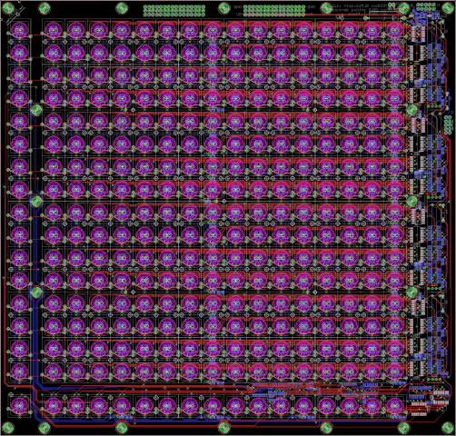
If I remove slave core3 and put slave core4 into the third spot, leaving fourth empty, then I do not get errors and just "SID3 not available". To me that means the core4 area on the PCB has some kind of issue but I can't figure out what to look for. I do not see any lifted tracks or cold joints. Are the CAN components just in the small area around the PIC socket? Maybe I'm missing a jumper or something stupid like that.
How about if you put core 3 (or 4) into the fourth spot and leave the third spot empty? If it fails then you know that the fourth spot on the PCB has a problem.
Measure conductivity from the pin of the socketed chip to somewhere else on the PCB, it could be that the socket itself does not connect the pin to the PCB.
-
Is it anything to do with the device ID that was flashed?
http://www.ucapps.de/mios_bootstrap_experts.html -
Would the numerical order of options stay the same if the features were rearranged into groups? The documentation and countless forum threads refer to specific options/#, so it would be confusing to renumber or reorder these.
The options could potentially go into an editable config file for easier overview? Generally you settle on a particular configuration and touch it very seldomly.
-
With velocity bars there is more info displayed and the spacing is more uniform. The hyphen/minus as a spacer for natural notes helps to connect them; with spaces it is more confusing.
Do you really use those low octaves so often @anonyme-x22? If it bothers you, a workaround is to transpose either on the SEQ or your synth.
-
1
-
-
Epic MIDIbox -- well done!
-
You can leave off the USB, it's only an additional +5V power option selectable by jumper..
-
1
-
-
One way is to use the punch in footswitch mode, but that's not exactly the same. Unless Peter knows of another way, maybe it could work to have scrub+footswitch (punch in) also delete notes under the cursor when the sequencer is not running?
Also an idea is to allow an "off" footswitch setting, for example if you only have a mono footswitch.
-
For this, set up a note track on AOUT port channel 16
Note 16 DOUT drum gates/triggers
Notes to CV Channel #16 (C-1, C#1, D-1, ... upwards) will be redirected to up to 64 digital outputs of the DOUT chain. Each key number triggers an individual gate for 1 mS, accordingly this mode is predestinated for drum triggers. The used shift registers have to be defined in the MBSEQ_HW.V4 file (DOUT_GATE_SR1..8) -
MCP4922 was indeed developed for, so it could be a good start? It doesn't look like it has a serial output, so if you need more than 2 channels you need to run them in parallel with /CS lines. That is a good advantage of MAX525/MAX5500 or the TLV chip.
The midiphy euroceiver has an IDC header that may be attached to a "crimpable" DB-25 connector. So that way it can sit in the back of the case if you like.
-
Great that you got it to work!
-
Seems like the bootloader is also corrupted, so the next step is to connect through ST-LINK and try to reflash that way.
Please see here:
http://ucapps.de/mios32_bootstrap_experts.html -
MIOS upload shouldn't depend on the SD card but you can try to remove it when flashing. You could try the following steps and see what works:
0. Restart MIOS Studio
1. Configure USB ports and try to upload
2. Hold and keep the blue button pressed. Now you should be able to bypass any faulty code and jump straight to the bootloader. Try to upload the SEQ app.
3. If you can't flash properly with the boot hold button pressed, reflash the bootloader using the miniUSB connector on the other side of the Discovery board and ST LINK Utility. If necessary, first update your STLINK firmware.You can find HWCFG files here (first get the firmware flashed):
https://github.com/midibox/mios32/tree/master/apps/sequencers/midibox_seq_v4/hwcfg -
Hi Roel,
I honestly haven't looked much more into this over the past years. There is a basic hardware setup and I still even have a few PCBs left, but I am not sure about whether this is the right approach. I also don't see a huge amount of activity on MIDIbox, meaning the uptake might be quite low. I could never fully agree with TK. on the UI/usage and that probably demotivated further development.
Regarding SD card/ethernet, I have not tried to use both at once. The assigned "SPI/PHY" ports definitely conflict, so it might need more elaborate software handling.
Best,
Andy -
Hi Phill,
What hardware are you using? Please take a picture of the control PCB and the core.
For uploading, you have to restart MIOS Studio each time the MCU is reset. If you have bricked your core, you should try to reflash it. How you do this depends on the hardware you have.
Best,
Andy -
Not sure if this is the right place for Arduino...
-
Great that you learned the mysteries of compilation!
I uploaded your file to the wiki page too:
http://www.midibox.org/dokuwiki/doku.php?id=sammichsid -
Hello,
You tested all of the inputs before soldering the Matias switches right? ;-)
The encoders are not on a switch matrix like the buttons are, so my guess is that there is a short between the two boards. Try to see if any resistors or diodes poke through. You could consider desoldering the encoder and bridging the pins to see if it is related to that.
But you mentioned "press on the encoder"; do you mean the encoder push switch? That is connected in the matrix in the same column as SW23.
Diodes in that column (including on ENSW7) are connected to pin 9 of J2 and pin 5 of IC3.
The encoder itself is connected through J3 pins 6/7 then through the header to pins 4/5 of IC5. A short to the adjacent pin (serial clock) might explain things.Best,
Andy -
Congrats on a fantastic looking MIDIbox!
-
Modular grid has you covered!
-
In theory yes I think you can, but there is a post from @Phatline saying that it didn't work when he tried, so maybe it needs code changes (at least for character LCDs).
http://midibox.org/forums/topic/19377-multiple-2x40-lcds-on-lpc17-core-solved/#comment-180667
-
You have the pinouts in the wiki and it basically follows the "J15" layout. There are 4x /CS signals per IDC10 header.
I think you need to configure the MIOS bootloader for the number of displays that you require (x,y), then connect J10B to the core GPIO to generate a pseudo SRIO/SPI to derive the CS signals with MB_NG or your custom code. The "J15" SI/SO/SC signals are simply buffered and routed to the headers as shown.
using 4 dio pins as a 4 bit dac
in Design Concepts
Posted
Maybe check out http://www.ucapps.de/mbhp_aout_lc.html
I'm not sure what app would suit you best though. NG is probably the most flexible, depending on what you want to do.