jaytee Posted April 3, 2019 Posted April 3, 2019 On 3/30/2019 at 4:03 AM, latigid on said: Good work! After ~10 years of soldering with a conical 0.5mm tip, I have recently discovered the joy of a 1.6mm chisel tip. It really is night and day with SMT as you get great heat transfer to the flat pads (always heat the pad if possible), then apply 0.5mm solder to the pin et voilà! With a conical tip I always had to use the side of the iron for SMT and the heating was much more tedious. Still the conical tip is better for larger THT components, pots and jacks etc. I have both irons at hand and just plug what's needed into the soldering station :) I just got a conical tip for my iron after finally wearing out the chisel tip that was on there... I have the opposite experience: I miss my chisel tip for THT! I switched because I thought it would be better for SMT, but maybe that was misguided. Either way I think I’ll go back to chisel here soon. I wonder if it comes down to what you learned with.
latigid on Posted April 3, 2019 Author Posted April 3, 2019 To be clear, I mean one similar to the middle tip of this picture, not the one on the right. It does mean that you have to solder with the iron the same way each time. Maybe my old tip was degraded or my technique wasn't right, but I never could get things going using the very end of the conical tip, rather I had to use the side.
pat_00 Posted April 3, 2019 Posted April 3, 2019 Yeah I prefer the chisel tip for most things, except for the really small stuff. On to the next problem, I have moved forward to testing the DINs. Everything works OK....but SW9-12 (Matias) and SW17-20 (MEC).. no response there. I'm guessing it's one of the 165s? all the soldering on them seems OK. Any clues where to look?
jaytee Posted April 3, 2019 Posted April 3, 2019 The tip I had been using was sort of a middle ground between the one of the left and the one in the middle. Definitely a much finer tip than that middle one, but still with a distinct flatted chisel shape. I’m having the same kind of trouble with the new conical tip; it takes a bit more finesse to get it in a position for good heat transfer, but right now I’m only doing THT. Any clever tips (no pun intended) for good technique?
Againsistm Posted April 3, 2019 Posted April 3, 2019 5 hours ago, pat_00 said: Yeah I prefer the chisel tip for most things, except for the really small stuff. On to the next problem, I have moved forward to testing the DINs. Everything works OK....but SW9-12 (Matias) and SW17-20 (MEC).. no response there. I'm guessing it's one of the 165s? all the soldering on them seems OK. Any clues where to look? I had this problem too and fixed it by using more tin on the 2 joints on the board. Watch out burning the super leds!
Againsistm Posted April 3, 2019 Posted April 3, 2019 3 hours ago, jaytee said: The tip I had been using was sort of a middle ground between the one of the left and the one in the middle. Definitely a much finer tip than that middle one, but still with a distinct flatted chisel shape. I’m having the same kind of trouble with the new conical tip; it takes a bit more finesse to get it in a position for good heat transfer, but right now I’m only doing THT. Any clever tips (no pun intended) for good technique? Gullwing tip and flux pen ftw ;-)
latigid on Posted April 3, 2019 Author Posted April 3, 2019 7 hours ago, pat_00 said: On to the next problem, I have moved forward to testing the DINs. Everything works OK....but SW9-12 (Matias) and SW17-20 (MEC).. no response there. I'm guessing it's one of the 165s? all the soldering on them seems OK. If SW1-4 work, then the problem is on the sink side. Check IC2 and associated resistors T3, T4 and the resistors/diodes adjacent. Are all diodes soldered with correct polarity? Please post a picture with your question. It avoids guessing games and is more informative in most cases.
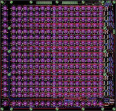
pat_00 Posted April 4, 2019 Posted April 4, 2019 (edited) Thanks for the tips, had a look and reflowed a couple of points, but no luck. Here are some pics of the areas you mention and the whole board. Edited April 5, 2019 by pat_00 pics not working...
Hawkeye Posted April 4, 2019 Posted April 4, 2019 @pat_00 could you try to reupload these pictures? The forum disallows attachments larger than a certain size (i think it is 1MB?), that's probably why the images come up as broken right now - so you might either need to reduce the JPG quality (not necessarily the resolution) in your image editor before reuploading here or you could upload them as they were on another service (e.g. imgur, dropbox, ...) Thanks and many greets! Peter
pat_00 Posted April 5, 2019 Posted April 5, 2019 Ok, I re-uploaded them at under 800kb each. Hope that works.
latigid on Posted April 5, 2019 Author Posted April 5, 2019 For the row of MECs SW17-20, you do actually have to solder in the switch that has the "sink bridged by switch" label on the silkscreen. The metal part of the switch provides the connection. For SW9-12 I don't know. Wrong transistor type maybe?
pat_00 Posted April 5, 2019 Posted April 5, 2019 Ah, that sounds like it could be one of my problems. Thanks.
pat_00 Posted April 5, 2019 Posted April 5, 2019 4 hours ago, latigid on said: For the row of MECs SW17-20, you do actually have to solder in the switch that has the "sink bridged by switch" label on the silkscreen. The metal part of the switch provides the connection. For SW9-12 I don't know. Wrong transistor type maybe? I have SW9-12 working now. But still no SW17-20 (on both LEMEC boards). All diodes are correct. Transistors too. Do I need to solder in the MEC switches? In the build video they are not soldered in and the testing works.
latigid on Posted April 5, 2019 Author Posted April 5, 2019 What was the issue with SW-9-12? To test the MECs on SW17-20, like I said, there is no connection unless that switch is inserted (just the marked one). It's the mostly likely explanation. Inserting without soldering might work if the leads scratch through enough of the oxidation that naturally builds up on the through holes and component leads. Or it might not.
pat_00 Posted April 6, 2019 Posted April 6, 2019 Not sure, I reflowed a couple of points here and there so that might have fixed it.
latigid on Posted April 6, 2019 Author Posted April 6, 2019 Okay. It's normally not an issue here but sometimes the boards benefit from a clean. It may depend on the solder/flux that you use. Do you use lead or lead-free solder?
pat_00 Posted April 7, 2019 Posted April 7, 2019 I use two kinds, both Kester brand. Both are leaded, one with a water clean flux and the other a no clean flux. I find the water clean solder flows much more reliably, but I was worried about the Super LEDs getting wet seeing as there is a warning about humidity exposure on the video. Also the no-clean solder leaves most of the joints looking dull like a cold joint, so this is annoying when it comes to diagnosing. Which is why I am reflowing things here and there without any real plan.
Smithy Posted April 7, 2019 Posted April 7, 2019 On 4/3/2019 at 6:33 AM, latigid on said: To be clear, I mean one similar to the middle tip of this picture, not the one on the right. It does mean that you have to solder with the iron the same way each time. Maybe my old tip was degraded or my technique wasn't right, but I never could get things going using the very end of the conical tip, rather I had to use the side. A genuine Hakko 936 style tip works wonders over the Chinese clones also, really worth spending the extra money one from my experience.
niles Posted April 11, 2019 Posted April 11, 2019 Quick followup on my SD Card not reading problem - Success! I was able to get the SD card to work :) It was something with the core board. No idea what it could be and not spending anymore time fixing it. Just redid the boards using new PCBs. The MCU was fine after all so now I have an extra for future projects. However....- I hooked up the JA board and loaded 'seq_l' program successfully in MIOS studio. However the LEDs and button activations are going haywire. I realized with slight horror that I used an older cable that I had made that was basically backwards. I have some extra HC595's from original mouser shipment and replaced the IC1 (directly under the SRIO IN shrouded header), but still getting the crazy led action. Good news is all the LEDs are lighting up and they are registering on MIOS studio, the encoder is as well. Bad news is they are just randomly flashing and activating on their own. Is there a schematic or pinout for this board so I know what I may damaged with incorrect cable? Could a bad cable have damaged the RN1, IC2 or IC3? Thanks!
latigid on Posted April 11, 2019 Author Posted April 11, 2019 Good to hear some issues are fixed! Please check the resistor network on the JA board is the bussed type (15 resistors), not the isolated type (8 resistors). The ICs may have been damaged with backwards cables. Pretty please a picture?
niles Posted April 11, 2019 Posted April 11, 2019 Just now, latigid on said: Good to hear some issues are fixed! Please check the resistor network on the JA board is the bussed type (15 resistors), not the isolated type (8 resistors). The ICs may have been damaged with backwards cables. Pretty please a picture? Ah ha - I must have just seen the '4816P' and so grabbed the bag with the wrong one. I installed the 1-103 in that location not the 2-103. I'll make that switch, hopefully I can salvage the one from the board, looks like I need it later on. Thank you again, I'll give this a shot and report back.
niles Posted April 12, 2019 Posted April 12, 2019 Well I replaced all the ICs on the JA board and the problem is less but still there. Now if I hold my finger on some of the pads on the back, the leds light up. I tried my other waveshare board and it's the same behavior. Attached a picture. Maybe I just order a new PCB and the specialized parts. Fingers crossed I didn't damage the main uCore board
latigid on Posted April 12, 2019 Author Posted April 12, 2019 (edited) Replacing the ICs also includes RN1? Are digital inputs now working properly (no random messages in MIOS Studio)? Quite a few of the joints look "cold." Did you solder the THT parts from the top or bottom? When you say 2 hours ago, niles said: Now if I hold my finger on some of the pads on the back, the leds light up. this results in the picture above? It's not too surprising if so, as the static from your hands can toggle the CMOS gates. That's typically not the best way to control 74HC logic though -- the static can also damage ICs. A picture of the rear would also be helpful. You can try to control the pins directly from the MIOS Studio command line with: set dout z 0|1 where z is from 0-15 on the JA board, 0 is low, 1 is high. Reset the Core, reopen MIOS Studio and don't load an _NGC file. http://wiki.midibox.org/doku.php?id=seqv4plus_jog has the matrix schematic. LEDs will light up if the the Cx column (dout 1 to 7; 0 not used for LEDs) is LOW and the Ay row (dout 10-15) is HIGH. Try not to light up too many columns at once. Note that it's not a proper scan matrix, so can be that multiple LEDs light up at once. Edited April 12, 2019 by latigid on
niles Posted April 12, 2019 Posted April 12, 2019 Yes-I replaced RN1. When I say I hold my hand on the back I mean that it's just very sensitive to touch. It's not like that with the other switches, just sw2,7,9,11,12,13 - they all act like one switch, one led. The only ones that are working as intended are sw3,4,5,6. The rest are dead switch/dead led. I usually solder THT components from the bottom out of habit. Attached a picture below of back. using MIOS studio as you suggested, I get some LEDs to light up. I can't follow which DOUT 1-7 and DOUT 10-15 correspond to which LED, it seems random. I tried reading the http://ucapps.de/midibox_ng_manual_ngc.html page about LEDs so I see that different combinations=different patterns, though unclear if that applies to this or the little matrix on the top of the board. Don't suppose there is a test script that would light up LEDs in sequence? One question I have is how does the chaining work with J89 and J89A? I see I have to connect the Left Lemec board into J89A on the JA board, would I be able to test the lemec boards if I just plugged the left board directly into the J8/9 on the core board? I am not sure if they are a direct connection or somehow buffered/filtered through the JA board first. I ask this because I just want to move ahead at this point (and see what else I screw up lol) and some of the pins aren't connected between J89 and J89A, which could be normal or not.
latigid on Posted April 13, 2019 Author Posted April 13, 2019 14 hours ago, niles said: Yes-I replaced RN1. When I say I hold my hand on the back I mean that it's just very sensitive to touch. It's not like that with the other switches, just sw2,7,9,11,12,13 - they all act like one switch, one led. The only ones that are working as intended are sw3,4,5,6. The rest are dead switch/dead led. In the post above you mentioned putting your fingers on the pads after you replaced ICs. The above statement makes that less clear; I guess you mean on the pads of the switches? Normally the pullup resistor on the 165 input should prevent this. With "less but still there" you mean you still get random triggers in MIOS studio? This suggests that the 165 inputs are still floating (multimeter on the pins should show about +5V), the 165 is damaged or the joints are cold. 14 hours ago, niles said: I usually solder THT components from the bottom out of habit. Attached a picture below of back. To me, the board would benefit from reflowing all pads, maybe with a bit more heat, perhaps cleaning the flux off especially around the ICs. 14 hours ago, niles said: using MIOS studio as you suggested, I get some LEDs to light up. I can't follow which DOUT 1-7 and DOUT 10-15 correspond to which LED, it seems random. I tried reading the http://ucapps.de/midibox_ng_manual_ngc.html page about LEDs so I see that different combinations=different patterns, though unclear if that applies to this or the little matrix on the top of the board. Don't suppose there is a test script that would light up LEDs in sequence? The activity matrix (16x8) is controlled by a different circuit on le mec_R. Back to JA, you should be able to "play" the LEDs with the piano roll (set as MIDI channel 3) in MIOS studio if seq_l.ngc is loaded. This might give you a hint if the LEDs are okay but the switches aren't. Other possibilities: cable is poorly assembled, try another and/or check for shorts on the pins. Pins 1/2, 3/4 and 7/8 are connected by design, but there should be no connections between rows. LEDs are not inserted with the correct polarity. Check the pins with a multimeter in diode mode. 14 hours ago, niles said: One question I have is how does the chaining work with J89 and J89A? J89 is the SRIO input, J89A is the output. J89A connects to the next board in the chain, be it le mec_L for a lefty or the line driver for a righty. 14 hours ago, niles said: I see I have to connect the Left Lemec board into J89A on the JA board, would I be able to test the lemec boards if I just plugged the left board directly into the J8/9 on the core board? No problem, just choose the _R.NGC when testing. In fact, I would suggest chaining JA -> le mec_L to see if the SRIO makes it out of the JA. As long as the power rails are okay, nothing else should happen. If le mec works as intended, then at least some of JA is fine. 14 hours ago, niles said: I am not sure if they are a direct connection or somehow buffered/filtered through the JA board first. I ask this because I just want to move ahead at this point (and see what else I screw up lol) and some of the pins aren't connected between J89 and J89A, which could be normal or not. It's normal as we need to shift the serial I/O on pins 5/6 through the registers. It works somewhat like a bucket brigade delay if that makes sense. You're doing great! Keep at it.
Recommended Posts
Create an account or sign in to comment
You need to be a member in order to leave a comment
Create an account
Sign up for a new account in our community. It's easy!
Register a new accountSign in
Already have an account? Sign in here.
Sign In Now