napierzaza
-
Posts
442 -
Joined
-
Last visited
Content Type
Profiles
Forums
Blogs
Gallery
Everything posted by napierzaza
-
Okay, thanks TK. My Encoder seems wired fine. Can you tell me what type of encoder mine is? PEC11-4220F-S0012 -Rear Facing -24 detents -20mm shaft -Insulated Shaft -Switch -12 pulses per 360 degree rotation There's a quadrature output table in the datasheet http://www.bourns.com/pdfs/PEC16.pdf I tried to compare it to this image http://www.ucapps.de/mios/mios_encoder_modes.gif
-
How about this one? I made it as "upside down" because I'm pretty sure you need to print it off that way because it's not pre-reversed like the underside in EAGLE. TOPSIDE.pdf TOPSIDE.pdf
-
1) Okay, taking the following two links: http://www.ucapps.de/midibox_fm/mbfm_frontpanel.gif http://www.ucapps.de/midibox_fm/mbfm_din_default.pdf Does "CFG Button" on the Panel equal "shortcut" on the DIN board? I cannot find any input called "CFG button" So am at a loss. My panels does not appear to really be reacting properly and I am testing all the wiring. 2) I have Detented encoders from Alps, I recompiled MIOS to be ENC TYPE 3, but when selecting instruments it sometimes just gets caught. Basically it just rolls through all the options until it reaches the end. Is there something I can do. My recompiled version, where all the encoders are type 3, is definitely a different MD5 than the provided .hex (and it uploaded fine).
-
Those are copies of the topside. But shouldn't the topside be mirrored? I may not. Hrrmmm. Also, I did never add the holes, because I could never find the right ones
-
I'm not sure what you mean, I looked at me PDF of the image and it was the same as yours. As for those PNGs, they are just screen captures to show what the board looks like. At any rate your posting is as good.
-
ACtually, I believe the dual-layered version has about the same amount of bridges needed if you're not making a double-layered board. However I guess it requires more drilling as the interconnections to the core would require holes (if using the SIL connector) EDIT: removed my copies for printing see below


-
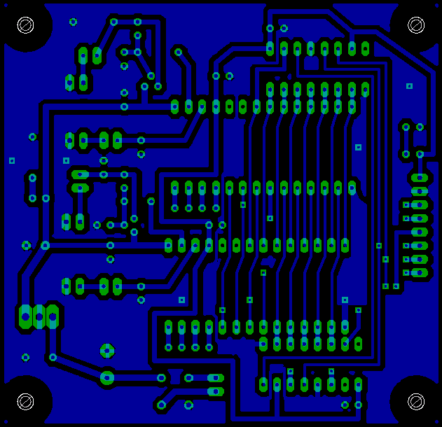
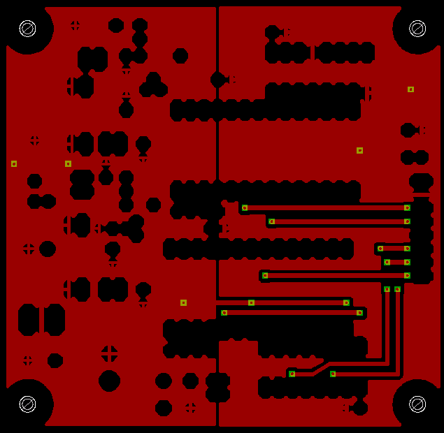
I had to clean up the single layered one a bit. Here it is. Double SID.pdf Double SID.pdf
-
I've never really understood how to do the ground if it's covered in a ground plane. So I make small 16 sized connections for them all, sometimes they're cut, but still maintain continuity and connection to ground via the ground plane. So I guess before you fill it looks a little messy.
-
So I think that's the final version above, note that both grounds are separated, and it's about 5x5.
-
Nope, you're mistaken! Look at the pages in the USB page.
-
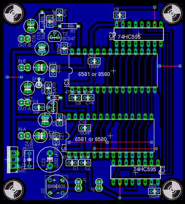
Hello, I have two 6851s and I am going to try and build a double SID module of my own design. I was going to build a SEQ so I have a lot of the parts already, but I realize that I'm missing a couple, pretty important, parts. Namely 4 Stryoflex caps (470pf) and 2 Transistors (BC547). I can basically re-purpose a lot of my other parts to work as I already have some DOUT 74HCs, and I believe the SIDs are as wide as the PICs, so I can just cut up some 40-pin IC sockets to work etc. So anyway, considering last time I had to pay 60$ to ship my stuff from Mouser, I was wondering if anyone here had just those parts that they could mail to me in Canada? I can pay you for everything, but it's just going to be cheaper if you stuff them in an envelope for me in place of having a box shipped. I'd also buy some SID IC-seats if you got em too.
-
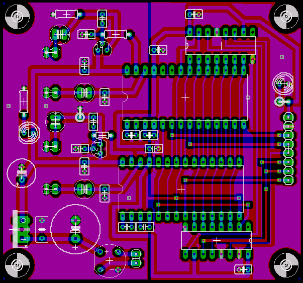
Thanks for the suggestions, I'm implementing them now, and giving the board more breathing room because of it. The caps were under the SIDs out of convenience, but I did move them out from under just cause it might save someone some time when building. I know there are dual sided boards, I just don't have any. I might just go ahead and work on a double layer design, but people would still have to modify the core. EDIT: Here it is, with a SIL Connector that should easily turn into a DIL J10 connector. I wish that I could make such a board. But anyhow it has most of your improvements. Now I just wish that I could make myself a double - sided one.

-
Here's an attached file of the board. I looked again at having a J10 connection, like maybe a SIL or something, but it is still really difficult. Basically you'd have to just do 6 jumpers to the connector, and would still have to modify the core. Here's a Bird copy of the board.
-
I guess it's possible, but it would require several bridges, which are just as time consuming as a direct connection underneath. And the J10 would not be completely compatible and the core would have to have one trace moved into another place. If it was a double-sided board it would be very easy and very nice, but I made it for myself, and I only have access to copper-clad boards. I wish I could have a smash board but I just don't have the facilities. The list of pins to connect are the following: Pin 8 (SID A) ---> Pin 24 PIC Pin 8 (SID B) ---> Pin 22 PIC Pin 6 (SID) ---> Pin 17 PIC Pin 12 (both 74HC) ---> Pin 23 PIC Pin 11 (both 74HC) ---> Pin 28 PIC Pin 14 (74HC A) ---> Pin 29 PIC
-
Hello, I have two 6851s and I am going to try and build a double SID module. I was going to build a SEQ so I have a lot of the parts already, but I realize that I'm missing a couple, pretty important parts. Namely 4 Stryoflex caps (470pf) and 2 Transistors (BC547). I can basically re-purpose a lot of my other parts to work as I already have some DOUT 74HCs, and I believe the SIDs are as wide as the PICs, so I can just cut up some 40-pin IC sockets to work etc. So anyway, considering last time I had to pay 60$ to ship my stuff from Mouser, I was wondering if anyone here had just those parts that they could mail to me in Canada? I can pay you for everything, but it's just going to be cheaper if you stuff them in an envelope for me in place of having a box shipped. Here's a pic of the board I designed based on Wilba's wiring. I excluded the J10 connection as I am going to just straight connect with a ribbon cable like the FM controls. The pins are way too splayed out to be worth while. EDIT: Removed one-sided .brd file as it is updated below MBHP-DoubleSID 2SIDED SIL.brd.zip MBHP-DoubleSID 2SIDED SIL.brd.zip

-
Thanks both of you. I certainly came across several references to files that did not exist in my search, but I should have seen them in the asm anyhow. Many thanks.
-
Okay, so my CS is working, but it goes crazy when I turn my encoder. I have a a Bourns encoder (PEC11-4220F-S0012) which is a 24 DET encoder. I'd like to change the encoder type but I cannot find the option at all in the FM source code. Where is it located? I grep'ed the whole folder and all I could find was some reference in "mios.h" which seems to be more of a decoding of what the options mean in a hex value. Further searching does not reveal any other reference to "MIOS_ENC_PIN_TABLE"
-
Okay, the answer to the question before was that Smash wants you to connect from J9 to the J1 port CLOSEST to the edge of the PCB, while he wants you to connect J8 to the J1 port FURTHEST from the edge of the PCB.
-
Okay, So now I've completely swapped out the DIN. I changed the entire board, all the chips, and the cable going to the hardware. This means that either the default .hex has nothing about a DIN module, or that my core has those pins burned out? I check the connections on my core and they're very simple traces that I made sure to redo. It still does not work at all.
-
Heehee, you actually deleted the wrong one, anyhow I'm not sure it matters. I just hope Thorsten reads this thread, please take a look at the reply-before-last that I made. As I have some answers to TK's questions.
-
Yes, please delete this one. I tried myself but I don't have permissions
-
I checked the continuity of the 5 wires to the core module and everything checked. Also I checked for the available voltage that was going to the module (4.9 volts). In terms of uploading MBHP128 I tried but for some reason my unit freaked out and the LCD had a bunch of garbage on it for some time afterwards. It stopped messaging when it booted up and I had to re-flash with MIOS and then the FM application. I'm a little bit anxious about doing that again. I figured I could just check it some other way, such as shorting the pins directly on the DIL to make sure it wasn't my buttons or button wiring. I got the a,b,c,d addressing from the jsynth snapshot that you have for download. When uploading the preset patches it only gives the options of a,b,c,d in place of the A0,A1,A2,A3 that I expected. I had wired the bankstick board just like the bankstick board said. I have read the description in the preset zip file and I believe it may have worked as I haven't gotten any errors. The only question is whether a,b,c,d meas a0,a1... Once I have my CS working I'm going to be able to actually navigate to the banksticks and troubleshoot that part.
-
I have checked my DIN Connections and everything traces fine to the core. For some reason there is not a single button that I can push that causes any change on the LCD. Are there additional things I should upload to tell the FM that there is a control surface? Also what are the bankstick.hex and bankstick.syx ? Are these the same files which can be loaded in the two different methods (ie they're encoded for mios loading etc)? OR do I have to load only one type? Using jsynthlib and it's supposedly working. How do I upload the 3 default presets onto my 4 24lc512 banksticks? Is the addressing A,B,C This is the equivalent to A0,A1,A2 for the banksticks? It plays every preset as it loads each individual one, but I am unsure how to make it switch to those specific instruments. It's also ambiguous whether there would be an error in the application if it failed. Strange thing is that I've checked my connections with a multi-meter to J9 and everything is good. The Synth starts up fine so I'm guessing that a short is not happening. I've even tried just tripping the main selection wheel with some pliers to make sure it's not my panel wiring and nothing happens. I'm starting to think it's the board or the ICs or something but am not sure how to check that. It's a smash board and I've looked over my work several times. I've removed all but the first IC to see if it works then but no luck. Which port of J1 am I supposed to connect my cable to (Smash DIN board)? The one nearest the edge or the one furthest? NOTE: This was in the MBFM forum but no one responded.
-
bump Strange thing is that I've checked my connections with a multi-meter to J9 and everything is good. The Synth starts up fine so I'm guessing that a short is not happening. I've even tried just tripping the main selection wheel with some pliers to make sure it's not my panel wiring and nothing happens. I'm starting to think it's the board or the ICs or something but am not sure how to check that. It's a smash board and I've looked over my work several times. I've removed all but the first IC to see if it works then but no luck. Which port of J1 am I supposed to connect my cable to (Smash DIN board)? The one nearest the edge or the one furthest?
-
The USB module is just like those 2 port (2xin 2xout) midi-usb converters. You can just wire them straight to the 2 cores instead of using any opto-isolaters and it works in Mac OS X without a hitch.