latigid on
-
Posts
2,524 -
Joined
-
Last visited
-
Days Won
149
Content Type
Profiles
Forums
Blogs
Gallery
Everything posted by latigid on
-
Maybe your issue is actually on the sink side, where multiple rows are triggering at the same time. With the NGC loaded, with your scope you should see the 595 outputs on IC3 (pins 15,1,2,3,4,5,6,7) toggling high in a sequence of 8. The pins correspond to A B C D E F G H where A controls the first four encoder switches, B the second four encoder switches, C the first four Matias switches...G the first four MEC switches (note SW19!)...
-
If you remove the seq-plate do you get the same behaviour? That would rule out clearance problems. ICs 1 and 5 scan the encoders (no matrix). ICs 2 (sink side) and 3 (DIN side) form the matrix for switches. Pins 11,12,13,14,3,4,5,6 of a 165 shift register are the inputs. If you don't read a voltage, probably the contacts in the encoder are connected to the common (0V) pin. Turning the encoder will change the state of the 165 inputs. You should also test the switch behaviour on IC3 in this way (first column pin 11, eighth column pin 6). I.e. test a switch in column 1, check that the input on pin 11 toggles low and high again. Check that the other inputs do not toggle. With your scope you can check pin 2 (clock, I think it's 1kHz) and pin 1 (strobe/latch, triggers after a certain number of clocks). Pin 10 is the serial data input that comes from 165s further down in the chain, pin 9 is the serial output that shifts data to the MCU or the previous 165 in the chain. Pin 15 should be at 0V. Did you already check if any adjacent pins of the ICs are shorted? IC2 could also be tested without the matrix running. Restart MIOS studio and don't load an NGC file. If you can be careful enough, you can try bridging the 165 inputs to 0V one at a time. Monitor the console data output. You could also use set dout x 1 where x is the 595 output to control sets of 4 switches without using a matrix, but maybe this doesn't clarify the problem.
-
Are the note events always the same, no matter what switch is pressed? I can't see any of the parts designators, so I can't help there. It's a bit fuzzy, but the solder joints look rough rather than smooth. So maybe some cold joints are there. Maybe try a slightly higher iron temperature? The JA board not being connected doesn't affect things. Are you sure you have seq_r.ngc loaded? As you have a working le mec, you can compare voltages on IC2 and IC3. Note any differences.
-
Backwards 165 IC or resistor network maybe? Bad cables? Transistors/diodes interchanged or wrong type of transistors? Pic of the PCB?
-
Probably SW19 is not soldered? Check for continuity across "bridge" marked with silkscreen and solder the pins or temporarily bridge if needed.
-
At a guess, some of the components from the seq-plate are shorting out those on le mec. The usual offender is the encoder right above the J89A header, but it could be more around IC3 on le mec, e.g. long diode legs from above. Check the diode orientation too. The note numbers from your output can be used to trace events in the NGC: D#2 = note 39 D#4 = note 63 D#6 = note 87 They correspond to the fourth column of buttons, pin 14 of IC2. Check the sixth pin (counted from the left when looking at the top of the seq-plate) of the 10-pin header J2.
-
-
Nearly there! The blood sweat and tears will make it all the sweeter!
-
The mini USB shouldn't have much to do with the +5V power, and it could be a dodgy pin contact (the PWR 5V pin as Peter noted) that reconnects when you put pressure on the board. A little note on connectivity tests: if you probe for connections between +5V/0V lines, you may get a short "beep" as there are capacitors that charge up temporarily. A short circuit on the +5V lines to 0V (which is quite nasty for your USB power supply and probably other components) is only diagnosed as such when you get a continuous beep or 0 ohm resistance.
-
Could you check the value/number written on R33D? It does look a bit like an initialisation error. Often this is to do with R33D, hence it is a lower resistance to make the pull-up "stiffer". Reflowing the resistor shouldn't affect the connection between PA8 and the OLED. Hence it could be something like a cold solder joint or unintentional connection to 0V on R33D, or an intermittent contact on the female header.
-
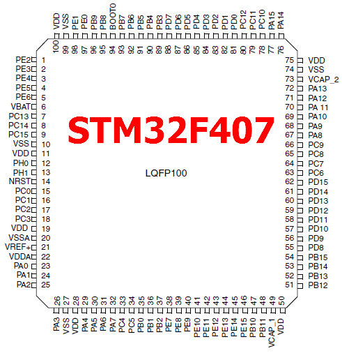
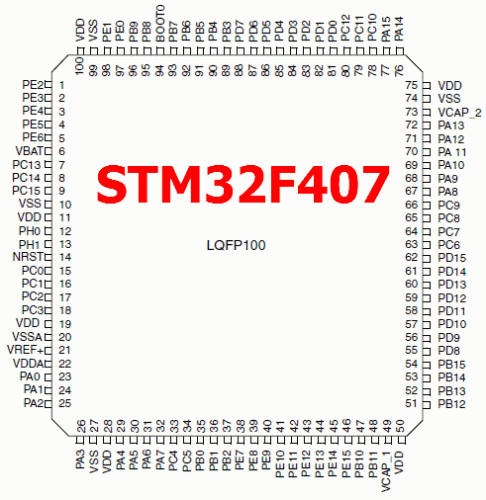
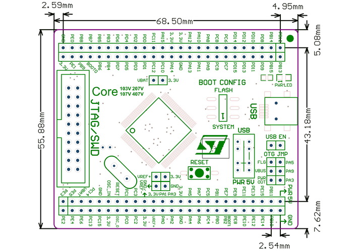
I confess that I'm not 100% sure about how the driver works here. It could be that the data edges are positive-going, meaning the MCU pin drives low for most of the time. This you could probe with your scope. As the displays work when plugged into the other J15, this would seemingly rule out problems with the OLED itself or cables. Meaning that it's further upstream. I would trace the E lines back to PC8 and PC9 on the v407 breakout (the header pins are labeled), and also back to the MCU pins. It could be that you have a weird contact on the female header for example. https://www.waveshare.com/core407v.htm https://www.waveshare.com/wiki/Core407V https://www.waveshare.com/w/upload/5/58/CorexxxV-Schematic.pdf
-
Next two things to try: check that all required lines are correctly pulled up to 3v3. These are RW (R33A), E2/E1 (R33B/C) and RS (R33D, 560R). All of these pins should be at 3v3 when powered up. Always take care not to short pins together on the OLED when probing! If you don't have another cable/headers around, you could try to use the SD card one (J16E; the application should start without an SD card). You'll probably have to bend the metal parts holding the display in to remove a cable. It could also be worth tracing the signals back to the MCU pins.
-
Mirroring is very confusing. As you have identified the +5V (unused backlight) and +3v3 (OLED power supply, J15_S is correctly jumpered), you can orient yourself this way. I don't think I was clear before: with everything plugged in (power off), check for continuity between the two OLED headers, i.e., left OLED pin #1 with right OLED pin #1 and so on. Also check the adjacent pins within one header for shorts, especially on the enable lines.
-
DSA clears: spider-approved!
latigid on commented on latigid on's gallery image in Schematics and PCBs
 She was pretty fast! I took the bag to the window and tilted it over and she jumped out super quick!
 -
LRE 4x1 breakable RGB LED-Ring/Rotary-Encoder PCB bulk order
latigid on replied to weasel's topic in Bulk Orders
The LEDs are quite cheap in bulk, the real cost here is the PCBA. But it is required for such LEDs as there are no pads to solder (they're underneath the LED dies). Plus, reflow soldering of these parts is notoriously difficult and it is very important to control the humidity to avoid lots of dead pixels. There are other projects around e.g. from @Antichambre and midiphy (myself) that are based on a similar concept. -
If you haven't done so already, place a bit of tape or even plastic or cardboard between the IDCs and the OLED PCB. Strange! It might be something to do with the E(nable) lines of the cable, so one display is updating with both displays' data. The schematic is here: http://ucapps.de/mbhp/mbhp_core_stm32f4.pdf Note that the pins are "mirrored". If you check J15A/B, you'll see that all pins are common between the two, apart from the E lines. With the power off but everything (except the USB cable) plugged in, use a multimeter in diode/resistance/continuity mode to check that all signals are common between the corresponding pins of the OLED header, also that no adjacent pins are shorted within pin columns of a header. Especially check the enable lines are not shorted to adjacent pins or to each other! Pins are arranged (view from the top of the display) 02 04 06 08 10 12 14 16 01 03 05 07 09 11 13 15 so you need to test e.g. pin 09 for shorts between 08 and 10 etc. From your previous posts, I think the LCD type is correctly configured (plus I believe the SEQ overrides the bootloader setting), but it could be worth uploading the bootloader app again: http://ucapps.de/mios32/mios32_bootloader_v1_018.zip MIOS terminal commands are: set lcd_type 0x02 store then restart MIOS Studio and upload the SEQ app again.
-
Check R33D (560R not 1k), check the IDC cable strands don't contact the rear of the OLED PCB. Swap cables to rule out bad cables.
-
Exciting! Best of luck with the rest of the assembly.
-
Hello and welcome! Glad that you're interested in the SEQ v4+. The functionality is fairly much as before, just the interface is a bit flatter. The obvious difference is the JA subassembly selects what the second row of Matias keyswitches does. But even here there is some familiarity, for instance the tracks are still in "groups" of four with the currently active track coloured differently. Labelled buttons are also almost the same. For sure, take any SD card. The one on the BOM is just there for posterity -- we don't expect anyone to order it from Mouser. Even if you have some old ones lying around or in an old camera they should be more than enough. Let us know what cards work and or if you have any trouble.
-
I can't remember if any of the encoders are mapped to anything. SEQ app or still with _NG? You can also check if any of the components on the SEQ-plate/lemec short out unintentionally. Normally the issue is with the encoders above the J89/J89A headers. The through-board connectors might also be worth a look.
-
Should be 17: SEQ les mecs, JA = 6 SEQ Core J4A, J19, J11E J19 = 4. J4B is also not required for a SEQ. Line drivers = 4 (can skip the Receiver if you'd like to build a Euroceiver later) I2C = 1 MIDI8 = 2 (could skip J2) Where are your 18 from? Core kit BOM says 11, UI kit says 6.
-
-
DSA clears: spider-approved!
latigid on commented on latigid on's gallery image in Schematics and PCBs
POIDH people! Save @jaytee!! -
@SimonSays I think as long as you have 4x virtual USB MIDI ports, the naming is not so crucial. It could be worth flashing the bootloader again. But it seems that _NG is successfully loaded and that SD reads work. Sometimes an SD format can also help. Possible causes of random DIN events: IDC cables incorrectly assembled (wires shorted together or missing, connectors around the wrong way) resistor network isolated type; bussed type is correct (ruled out) resistor network incorrectly oriented shorts between IC pins check pins 6/7 as there seems to be some flux/fluff/solder splash etc., also elsewhere on the board. Floating IC pins: check 165 inputs (pins 3-6, 10-1) are at +5V. IC damage from static or overheating.
-
Hello, First thing to check is if you have soldered the correct resistor network on the JA board? Second, I think you don't have MB_NG flashed onto the Core? Maybe the SEQ app is flashed?