latigid on
-
Posts
2,524 -
Joined
-
Last visited
-
Days Won
149
Content Type
Profiles
Forums
Blogs
Gallery
Everything posted by latigid on
-
The JA matrix is driven by the extra ICs on lemec_R. The fact a whole row is missing points to an issue on the sink side. Check continuity (also for cold solder joints and faulty cables) from the following pins lemec_R: IC17 pin 1 :: IC18 pin 7 IC 18 pin 12 :: J5 pin 8 J5 pin 8 ::IDC cable to JA:: J2 pin 8 JA: J2 pin 8:: MATRIX pin 14. The matrix pins are labelled like an IC, so anticlockwise from the bottom-left dot.
-
Do the DIN tests work? I.e. do you see button events in MIOS Studio? The problem is isolated to one LED, not a whole row-of-four or column? Then the issue is soldering to that particular part All LED anodes/SJ of a column will be common, test continuity You have multiple colours configured? Check the RJs. Provide a few good-quality photos to make troubleshooting easier.
-
Maybe create another post as it's not really a v4+ problem? Could it be the HW config settings or an issue with midi loops feeding back in? More than one track assigned to AOUT? The perennial IDC cabling issue would also be worth checking.
-
LRE 4x1 breakable RGB LED-Ring/Rotary-Encoder PCB bulk order
latigid on replied to weasel's topic in Bulk Orders
@TK. thanks for the coding efforts! This will be very helpful in other projects too. The rainbow rings look very pretty :) -
We should get panel samples in a week or two, then do a PCB run. Still a wee way off.
-
The caps are not to my taste, but good for you if you are happy with that look :).
-
The activity matrix? Check the HW config file as you need: # set to 1 or 2 to enable the relative track position display # 0: TPD disabled # 1: TPD enabled - columns are cathodes, rows are anodes # 2: TPD enabled - columns are anodes, rows are cathodes # 3: TPD for midiphy frontpanel enabled - columns are anodes, rows are cathodes, inversion TPD_ENABLED 3 De rien! You had a great attitude and provided the right info (pictures). It's really great work if it's just your second project! Félicitations!
-
Each display gives this output when only one is plugged in? Then the cables are okay, or at least have the same issue :). At a guess, probably the register data is corrupted, so look again on IC2 for cold joints or shorts. Make sure the power is jumpered to 3v3 (it was before I know). Check that the 407v board is correctly inserted into the 2x 2x25 header pins. You may have bent the connectors by inserting/removing the 407v a lot. Reference the schematic here and check for continuity back to the top of the 407v header pins PD7, PD6 etc. Check that the E (enable) lines of the displays are not connected together.
-
Make sure you clean up all of the pads (with desoldering braid) before resoldering IC2. Pin 16 can be bridged directly to C2, no problem.
-
The soldering on the OLED headers could be better, try to rework. If the fillet looks like a teardrop, it might not be contacting the PTH properly. Try to get the heat into the pad and the solder will flow there. Soldering could be better on IC2, pin 8. Recheck R33abcd. Try swapping the OLED cabling to the other J15 port. Could be bad cables again, could also be that some pins on the cable short out components on the OLED, so isolate with even a scrap piece of plastic or card on the OLED PCB right under the connector.
-
That might be a hard combination to tune. But yes, normally blue should have a lower-value resistor as it's typically dimmer. At least on the older SEQ firmware, the measure LED was not "XORed" i.e. beat and measure would trigger at the same time. That might be a way to get all three going at once for white-ish, though I can't remember if it's still part of the current firmware.
-
[SOLVED] SSD1306 again. Help an idiot find his mistake please.
latigid on replied to weasel's topic in MIDIbox NG
Sometimes I feel like there can be oxidation or other crap on the pins that prevents good contact and messes up the data transfer. -
-
If _NG is flashed and JA is working it's a good sign. The _l and _r .NGC files specify the position of JA. You can use _r to test lemec_L. It's possible to test lemec_R as the first board in the chain, but you need to reconfigure the file. The boards are chained JA-lemec_L-lemecR, correct? You should measure +5V on the 74HC165 input pins and 74HC595 outputs should go to +5V with set dout all 1. Check the preceding pages of this thread or the datasheets for pin assignments. You can follow the SRIO chain (especially the SO signal) to see how far the data gets. Seeing as you have some DIN activity, consider replacing IC2/IC4, which were reversed and then heated up probably quite a lot during rework.
-
Just check first that the MB_NG app is flashed and you have loaded the correct seq_l or seq_r.ngc. Was testing of the JA board okay? To simulate DOUT behaviour you can try set dout all 1 Or go through and count the dout pins (8 per chip) until you get to the correct IC -> replace all with the one you want to toggle. DOUT rows/cathode sink rows are given in previous pages. The matrix is controlled by ICs 2 (cathodes) and 3 (DIN). Having spare parts is always useful and could be used in future projects. I typically get 100 shift registers at a time.
-
No worries. It might be that IC2 was damaged by being reversed. Did you use new chips or the same? I was troubleshooting with @niles the past weeks on a similar problem. The same advice applies, so check cables, resolder IC2 and IC3. Many solder joints look "cold" Any MIOS output with set debug on ?
-
When you say the "kernel" doesn't boot, do you mean the waveshare MCU breakout board? If this is the case, a typical cause is a short between 0V/+5V. Please check the orientation of all ICs. At least IC4 is in backwards! (The stripe on the IC should go towards pin 1).
-
Glad you got it working. Interesting solution, as R33A is more associated with the OLEDs.
-
Frequency is controlled by the CPU, I'd say if you see the clocks at all it's good. It might be that RC is 1 kHz. How's your DIN matrix looking?
-
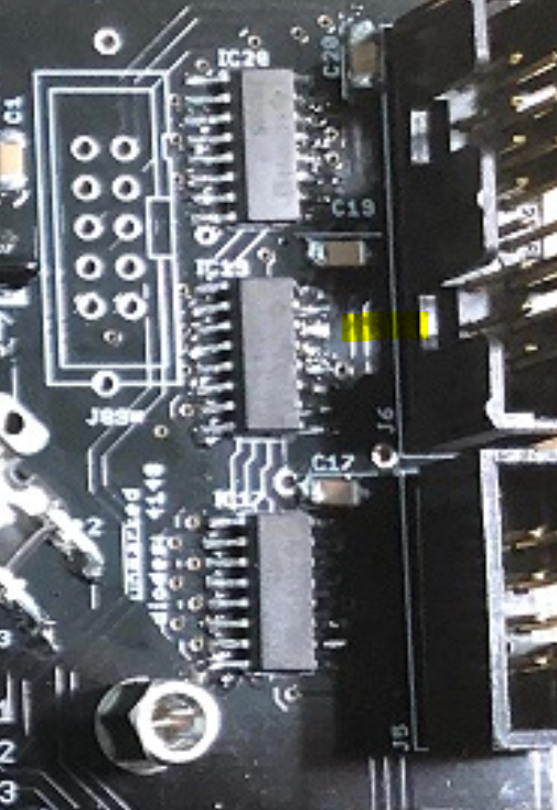
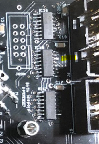
R26 is connected between 0V and pin 13. If pin 13 is at 0V, it's a good sign. Perhaps the serial data doesn't make it to IC2. Actually ICs 17, 19 and 20 are before IC2 and finally IC4 in the chain. Scope the same pin 14 on each IC to see how far it gets. You can also check for continuity between the following points: J89 pin 6 (middle pin, other side of the notch), IC17 pin 14 IC17 pin 9, IC19 pin 14 IC19 pin 9, IC20 pin 14 IC20 pin 9, IC2 pin 14 Looking at your picture, I can see a probably cold joint on IC19, pin 14.
-
Sometimes OTG devices don't play nice together. We're still learning what works and what doesn't. Did you adjust the Keystep jumpers for USB sync?
-
I think you've ascertained that the DIN side is good. Thanks for the tests! The sequence of outputs on the 595 just goes around in a cycle. It toggles one output high, which turns that transistor "on". Meanwhile, all other outputs are low, so all other transistors are "off". Then the next output goes high. By turning on one transistor at a time, you enable only one row to be scanned (here only four switches). This is how you differentiate between switches in the column of (here four). It makes not difference if any switch is pressed; the 595 outputs cycle like a background task. The fact that you see (or saw) all four switches triggering makes sense, as your 595 outputs are all high, rather than 1/8 each time. So I suggest paying close attention to IC2 again. E.g. it looks like pin 8 is not soldered properly? It is actually possible (hopefully not, but a possibility nonetheless) to damage CMOS by sending it data while the chip is not properly powered. If you compare IC2, pin 14 on both boards, you should see a similar pulse train that is offset by (I think) 24 clock ticks. Pin 12 should toggle at the end (and I think also at the start) of the pulse train. Check R26 is properly soldered and that pin 13 of IC2 is ~0V.
-
It just interrupts the +5V supply on the USB A socket. I don't know the workings of a Keystep: can you power it externally?
-
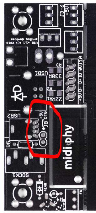
First thing: did you connect the jumper on the USB PCB?

-
@Simon Sounds like a sync issue, probably not related to the build. Please explain your setup, what sync and routing settings are used etc. Maybe in a new thread? Thanks for the beer the other day btw!