latigid on
-
Posts
2,524 -
Joined
-
Last visited
-
Days Won
149
Content Type
Profiles
Forums
Blogs
Gallery
Everything posted by latigid on
-
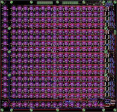
Here's a souped up version (intended for Programma): All registers on board. 45 degree styles Room for OLEDs Individual touch sensors, wired to encoder bodies at the moment. A bit hard to capture the LEDs, but I hope you get the general idea. The touch sensors are set to activate the LEDs and they can be "dimmed" using a MIOS CC value. It's very preliminary for the moment, but eventually the idea is to use the touch sensors to turn on the acceleration function of encoders. That needs a bit of thought though.
-
Hello, sorry but what's NRPN? The key to this (potential) issue is whether a USB host connection from the computer is required to boot the STM32F4 on later revisions. For your standalone case, how is the board powered? If it's via a computer, then I guess the USB connection is still present?
-
Either side of the duo LED (3-pin). or Erthenvar etc. I think Mouser might even stock them. Anyway, they're very widely available.
-
Op amps are pretty good amplifiers :) TL07x are quite good "Swiss Army knife" chips and you can generally make an amplifier, mixer, inverter, filter etc. with just a few external components. Depending on where the audio is going, you may want a decoupling cap in there to remove DC offset. ... While I'm here, these are the current PCBs for the "CV toggle." I decided against the toggle switches, because they're too big and you have to pay ~$5 each for decent quality ones. Tayda have cheaper options but they're generally not well regarded. I've opted for push button DPDTs instead; because a centre-off (ON-OFF-ON) isn't possible, I used two per channel and the second pole is used to illuminate an LED, which effectively tells you what range setting you're in. I was also unhappy with the mounting -- too much space and the 90 degree ribbon connectors were awkward. Now the whole thing is 50mm wide with the processing board stacked below the panel board.
-
The idea is you use: one Control PCB + one AIN -- OR -- one Control PCB + one AOUT (you can't use both in the same "sandwich") The Control is flexible in that in can be configured for either; you stuff different resistors/diodes/solder jumpers, while the SIL headers connect to different parts of the respective PCBs. Yes. Plus a some sort of DOUT (e.g. SmashTV, MBCV v2). MAX525. It is expensive but has proven itself as a good DAC. I soldered two AOUT_NG modules, one doesn't work and for the other, channel 1 is non-linear viz. my SEQ tuning. I don't know if that's a problem with the chip; maybe I overheated it whilst soldering?? But checking on Mouser, MAX525 is one of the cheapest DACs available in DIP. There are a few others, but I couldn't find many (any?) with serial out (Tx). It's still listed in active production and if there's sufficient interest maybe I can look at a bulk order. I'd also like to chat with TK. about a possible MUX/DEMUX board. Thus you might have 32 (64?) inputs for ADC and 32 (64) outputs for DAC using SMP08s, and a 74HC595 to generate chip select addresses. Best,
-
 Control + AOUT + DOUT stacked.
 -
This is a general interest/info post for a new(ish) CV concept. The green PCBs are 4 channel AOUT and AIN boards. Either one stacks with one blue "Control" board. AOUT: MAX525 based. I realise that @Altitude also has an AOUT in the pipeline, so I want to explain the pluses for both. @Altitude 8 channel more compact (minimum rack real estate) DOUT onboard lots of clocks and triggers US shipping @latigid on more spacious (a bit more ergonomic) switchable ranges (0-5, 0-10, +/-5V) manual fine tune control through hole assembly (no fine pitch SMT) new amplifier circuit with precision references and compensated outputs EU shipping matching panel design with AIN (see below) Status: I have most of the parts on hand, so this should be tested within a few weeks. AIN: switchable ranges (0-5, 0-10, +/-5V) to optimise ADC levels protection against overvoltage (op amp limiting) attenuator -- can set to clip the op amp input for interesting CV shapes! normalisation of the inputs to +5V -- can use pots as manual CV sources 3v3 power from a Core or an onboard Vreg Status: tested as working from an older proto. Waiting on a few parts to complete it. Control: Eurorack compatible Accepts either "Thonkiconn" (PJ301M-12) or PJ301BM jacks 4 channel AOUT or AIN 4 channel gate/trig/clock with LED LEDs are driven from a Schmitt trigger so shouldn't interfere with your power rail 1 clock can be set as an input with CV protection and conditioning (even works with a sine wave!) this conditioned clock can be sent to a Core e.g. MBCV DPDT (7mm) switches to engage the range functions: switch in a resistor to adjust gain settings switch in an offset for bipolar operation (you could have +/-2.5V or even +/-10V if desired) Duo LED to indicate current CV range configurable adjustment pots fine tune with diode deadband for AOUT attenuator for AIN note: the 9mm Alpha pots fit, but I have some "long shaft" versions on order. They have a knurled shaft and pointer which doesn't require a knob. mounting for a DOUT R5 board (see below) Status: needs to be tested with the AOUT and AIN boards, but the mechanical fits look okay. ^^ just thrown together, I suppose shorter standoffs would be possible. My design goal for an MBCV example is 2*AOUT and 2*AIN: 8 CV out 8 gate 8 CV in 7 clock out 1 clock in You'd have 200mm of PCBs, which is around 40HP of Euro space. I expect boards could cost 5-6 EUR each.
-
From the album: AOUT + AIN + EURO
© 2016 latigid on
-

From the album: AOUT + AIN + EURO
© 2016 latigid on
-

From the album: AOUT + AIN + EURO
© 2016 latigid on
-
POIDH!
-
Hi Matthias, What's the version number printed on the Discovery board? Did you try removing the solder bridges as detailed in the post above? Best,
-
Hi Zam, Okay, is the D variant working whilst plugged into a computer or standalone? Best,
-
For interest, can you post the version number silkscreened above the ST logo (topside)? MB997C seems to behave okay, while it looks like MB997D has problems with the bootloader if a USB host isn't present.
-
Seems like there is a problem (when a USB host isn't connected to the Discovery board??) Try to unbridge those connections and see if it helps. Also it would help if you listed your version number.
-
Problems running app on new STM32F407G-DISC1 pcb
latigid on replied to illogik's topic in Testing/Troubleshooting
I have an STM32F4 board (about a year old from Mouser) with MB997C above the ST logo on the topside. My newer Disco boards (a few weeks old from RS) have MB997D. I haven't needed to test these yet, but I found a thread that may be of help: https://my.st.com/public/STe2ecommunities/mcu/Lists/STM32Discovery/DispForm.aspx?ID=15970&RootFolder=%2Fpublic%2FSTe2ecommunities%2Fmcu%2FLists%2FSTM32Discovery%2FSTM32F407G-Discovery-STlinkV2(V2.J25.M13)%20%20-%20Boot%20fail%20using%20external%20power%20supply Hope that can be of help. -
I don't think so, but from memory it uses a PIC. I don't have personal experience with scanning pots into MIOS, apart from the BLM 16*16+X. AINSER(X) is the external ADC solution to expand the AIN capabilities but I don't know about the performance (try searching the forum). PICs in general have better handling of analogue inputs; this is why they are used as part of the MF_NG module. Then again, Mutable Instruments uses a single ADC pin and four multiplexer chips to scan 28 pots in Elements. I know from using the module that some parameters are definitely lower resolution, e.g. the tuning controls are quantised.
-
Only you can decide that. My perspective on pots is that they make less sense on architectures with presets, like a universal controller. Of course you have relative/snap/absolute handling modes, but they don't beat the simplicity of an incremental encoder. Pots (also encoders) are subject to wear and dust and are inherently more difficult to scan. This difficulty increases with the number of inputs (slower scan rate etc.), although I'm sure TK. has routines for minimising jitter errors. If you're sending CC data rather than NRPN (well first we have to look at the effective resolution of the ADC), it's all quantised anyway. Pots also make little sense with lower resolution parameters. A prime example is the Rhodes Chroma ENABLER. Almost $4000 to have one built (a lot of wiring and parts) and some parameters have as few as 4 values. But it demonstrates that it can be done with pots if you choose. Finally the likelihood of a project being completed is inversely proportional to its size and complexity. Pimping the ELO (Programma) boards, this breaks the task down into smaller chunks.
-
Fair enough. Out of interest, how many pots are you looking to implement?
-
I think it would be possible to do a 4*20 display on a single OLED. Understand that the traditional SCS layout (visible in the MB CV control surface above) typically puts 4 buttons below the LCD to select menu items. You're describing the Programma. 1-4 ELO boards with sets of 16 illuminated encoders and 4 "labelling" OLEDs, auxiliary SCS-OLED boards for patch name, envelope shapes, SCS button labelling etc.
-
No worries, PCBs should be here today if DHL get their act together. I have white 0.96" OLEDs on the way, could possibly try with a yellow-blue I have left. The thing is, you don't have an ordinary button layout, so maybe traditional SCS LCD functions don't make sense anyway. But as far as the display goes, a 2*20 CLCD is 100 pixels across with a gap of ~1 pixel in between characters. So the horizontal resolution is comparable. I chose the 6 button "hex" layout just to try something different. My thought was that there's enough space to provide two menu rows of 3 items each. Have to see though, my guess is @Hawkeye will do most of the hard work with the Programma builds ;-). This gives an idea of how the text fits, approximately 20 characters:

-
Not yet.
-
Here's an updated picture: You can see 7 pin SIL rows for the displays and the six switches/encoder (two positions possible). Encoders with built-in switches are supported but you have to wire your own pins. Possible configs are: OLED OLED OLED OLED OLED [6 buttons] OLED OLED OLED encoder OLED [6 buttons] encoder only switches only encoder combo of switches + encoder fewer OLEDs Pinning for the OLEDs is based off J15A from the Core32F4, same for the display driver. Pinning for the SCS is the standard J10(A). It would be possible to split the SCS functions across two boards, e.g. with OLED [buttons] OLED on one and OLED OLED encoder on the other.

-
Some cool grooves in there! Aphex Twin fan? What's the synth/sampler setup?
-
Do you know if it's possible to have say 4x 128x64 OLEDs and 1x 256x64 OLED all with the same controller chips on it in a MBNG system without customizing the code? I don't know for certain, but at a naive guess I think you would need to program the displays with the maximum pixels in mind. So in your suggested setup you have five 256*64p displays, where the first four are only used at 50%.