

latigid on
-
Posts
2,524 -
Joined
-
Last visited
-
Days Won
149
Content Type
Profiles
Forums
Blogs
Gallery
Everything posted by latigid on
-
Software side is very easy, everything goes across MIDI over USB and the chips can be flashed without any extra programmers etc. http://www.ucapps.de/mios32_download.html It's then a simple process of choosing the correct application and keeping up with TK's constant updates! You may also need an SD card PCB, these are currently not available from AVIShowtech (SmashTV/Tim) but can be found on eBay and Sparkfun.
-
:smile: It's from days gone by where everything was Moog and Space Echoes! I've since moved on but kept the moniker. OP: SEQ V4 Lite is probably the simplest project to get going on, so if you can solder a few LEDs and switches you're halfway there already.
-
Hi, check out http://avishowtech.com/buy for the PCB, I think you have to source your own switches and LEDs though. Best of luck!
-
I think the pinout is different to start with, so you would need a custom cable or connector. Isn't the protocol completely different from MIDI also? Perhaps do a search for DMX on this forum, surely people have tried in the past but not with a 32-bit core.
-
Je pense qui les pots analogue motoriser sont chaque fois contrôlée digitalement. Donc tu vais besoin d'utiliser un PIC ou quelque chose similaire. Tu peux à regarder le module "MF_NG" pour les idees: http://www.midibox-shop.com/mf_NG.html http://ucapps.de/mbhp_mf_ng.html
-
Could take one or two, if they indeed work correctly.
-
 Quite strange sockets; any reason for this?
 -
Might have to block status updates, they're going crazy over there
-
Order from RS arrived. 6 separate packages including a 1m box containing an IC tube with 4 DIP14... CHF20 in parts; lucky shipping was free!
-
Surely it's the SEQ V4... seeing as that's the forum he's posting in.
-
Wilba's website is down, offsite doco = bad.
-

-
"Website suspended
The website you are trying to reach is currently suspended.
If you are the owner of mb6582.org, you should log in to your Toolkit or contact your hosting provider."
-

-
-
These are SIL (single in-line) headers, no? Just buy a row of 40 or 50 and snap/cut them to fit.
-
Mike :no: Tim est un membre de notre organisation depuis plus de 10 ans, il est digne de confiance ici Il est normal d'attendre une semaine pour une réponse, pense que si tout le monde lui-demande, il ne sera pas le temps d'envoyer les commandes! EDIT: I don't know why I keep doing that, sorry Smash. Perhaps European MIDIBoxer = Mike for me. :facepalm: On the other hand, feel free to go through Mike if you need something shipped from Europe: http://www.mikes-elektronikseite.de/
-
Protection: yes, definitely. The two systems used are buffers/level shifters (also gives you a +5 V logic level in the case of newer Core modules) and 220R resistors for short circuit protection.
-
Please explain your set up. Are you using the Wilba control surface? Do you have the SEQ running correctly? Have you edited the hardware config file?
-
No, what's your set up? Have you level-shifted the 3.3 V signal?
-
Just a thought here: J19 on the LPC core is already buffered, while on the STM 32 it isn't. This might make all the difference! Also, the pinning seems to be a bit inconsistent: J19: Vs Vd So Sc Rc1 J1 : Vs Vd So Rc Md TK : Vs Vd Rc1 So Sc The J19-J1 pinning is therefore not 1:1?
-
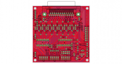
This revision has a connector for J19, for ocassions when the AOUT module is outside the case. The three data lines are buffered by a CD4050, unfortunately it's SMD as I couldn't find a part that would fit easily. One of the additional buffers is available, there wasn't room to route up the other two so they are tied to ground. The connectors share the same pins as J4 from the AOUT. EDIT: Pic
-
-
It might help if you list your location. Are these the two-piece PCBs which need wiring together?
-
Another approach: http://www.reenigne.org/blog/physical-tone-matrix/
-
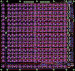
Maybe run the Eagle DRC? There are two vias which overlap and many traces below the minimum clearance. Best of luck!
-
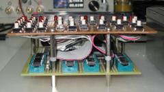
Good job, but I don't think that there are enough mount holes. These things are pretty long, covered in components and one would be applying pressure over the whole surface. Too much flex in my opinion.
-
I can squeeze in one more connector on the top left side for people who will send the signals from J19 to an external AOUT module. Should the three data lines be buffered also? This should be doable with an SMT chip.
-
Okay, I think I'm done now. I think that it looks okay but I'm not 100% sure on the regulator circuit. If somebody could check that would be great. Also: no answer as of yet on the MIDI IN/OUT 3 situation. In any case, I have brought out the 3.3 V and 5.0 V connections.