latigid on
-
Posts
2,524 -
Joined
-
Last visited
-
Days Won
149
Content Type
Profiles
Forums
Blogs
Gallery
Everything posted by latigid on
-
© 2014 latigid on
-
© 2014 latigid on
-
© 2014 latigid on
-
© 2014 latigid on
-
© 2014 latigid on
-
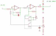
Okay, another concept but now it's for CV inputs for MBCV. Again I'm abusing centre-off toggles. The idea is to maximise the scaled signal input while protecting the ADC from over- and undervoltages. Each inverting gain stage should give a final input range of 0-3.3 V. The centre-off position is for 0-5 V inputs. The two stages are set for -0.66 and -1 gain. Note the (variable) resistor is out of circuit when the switch is in the middle position. The other two positions are configured for -5 to 5 and 0 to 10 V inputs. One switch pole adds a +5 V offset, while the other adds in a second resistor for both conditions. So we have two gain stages of -0.66 and -0.5, again giving a final input range of 0-3.3 V. The output of the second op amp is current limited and clamped between 3.3 V and 0 V. It might be useful to use BAT54S Schottky diodes as they have a low forward voltage (e.g. 320 mV at 1 mA, 400 mV at 10 mA). It might not be enough though as apparently the STM32F4 AINs shouldn't exceed Vcc (3.3 V). But Vcc max is 3.6 V? I'd appreciate some advice here. More current limiting? How are the ADCs handled on the STM cores? Are some bits discarded? Is it better to limit the voltage more conservatively? I thought about rail-to-rail op amp limiting (Vcc = 3.3 V) but it seems that most chips max out at 1 volt below Vcc. Reference threads: http://www.muffwiggler.com/forum/viewtopic.php?t=104872 http://mutable-instruments.net/forum/discussion/938/cv-inputs-how-to-protect-them-from-negative-or-too-high-voltages/p1 http://www.eevblog.com/forum/projects/pic-input-protection-using-a-zener-diode/msg21840/?PHPSESSID=33bbdf2e2a88957db87cce882680f1ca#msg21840 http://www.nxp.com/documents/data_sheet/BAT54_SER.pdf
-
-
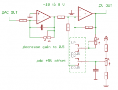
I am thinking about a control circuit for CVs in any one of the available AOUT modules. The concept involves a -10 to 0 V source derived from the DAC and an inverting amplifier. The second op amp stage can do one of three things: 1. Inverting buffer (voltage level = 0 to 10 V) 2. Inverting amplifier (voltage level = 0 to 5 V) 3. Inverting mixer (voltage level = -5 to 5 V) This would be accomplished by an ON-OFF-ON DPDT toggle switch. Case 1 allows the voltage to pass without any further change (middle position). The second switches in a resistor in parallel with the feedback element. Using a cermet trimmer, one can get an accurate gain setting of 0.5 for unipolar 0-5 V (or any other value up to 10 V). The third adds a trimmed offset of 5 V for bipolar operation. Should it work? Thoughts and criticisms are welcome. :)
-
-
Also a bit too big for my use also, sorry!
-
Possibly interested in one, depending on pics!
-
Really like this one Peter, keep it up!
-
Nice work!
-
Re: connectors, I guess it depends on which core you'll use! For the TTSH I have a gate booster pcb that also generates a trigger pulse kindly designed and routed/fabbed by people on MW. But I was originally thinking of similar oddball synths like the 2600 when I was playing with CV/gate breakout boards a year ago. It's still nice to have higher voltage available for non-Doepfer gear. My comment on voltage regulation was more applicable to systems with bussed power. If you have a regulated bipolar supply dedicated to this AOUT module, no problem. I hear that taking your VCO pitch reference directly from a power rail is not good design.
-
You should probably discuss this more in the HUI section of the forum, this part is for new design concepts.
-
Probably a good idea to start going SMT for small-scale applications! Can I ask why you have decided on the 525 as a DAC? Better linearity than the TLV5630? really progressed this year, I moved and now I'm occupied with Eurorack projects. But, I still plan on using a SEQ V4 and/or a with analogue outs. Maybe I was too optimistic about getting the power from the modular though and I'm toying with the idea of a larger (3U x 126 HP) SEQ case with outputs mounted topside. The idea of trimming the gate down from 12 V is a good one, it might also be a good idea to provide a regulated voltage for the offset control. as it makes bipolar trimming very difficult or impossible. Perhaps a 1:1 header pinning from the core could be useful if there's space? And you might also want to keep the digital and analogue sections of the PCB separate, which is harder than it sounds!
-
Hmm... 5-0 in one half
-
C'est trop cher!
-
Can you upload a picture with the ground plane poured? Some connections look a bit funny.
-
Did you correctly change the sequencer output to AOUT1-8? The default will be USB, MIDI, IIC etc. Failing that you could try the TEST AOUT PIN program from the Core, it should be somewhere on ucapps.de Bonne chance, Andy
-
Check your J5 and resistor network orientations too!
-
MB-LRE8x2CS rev 4.6 BULK ORDER spring 2014
latigid on replied to Fairlightiii's topic in Bulk Orders
Nice, have improvements been made with regard to LED saturation?