

latigid on
-
Posts
2,524 -
Joined
-
Last visited
-
Days Won
149
Content Type
Profiles
Forums
Blogs
Gallery
Everything posted by latigid on
-
From the STM32 core page on ucapps: "Pin mapping suboptimal in some cases. E.g., the outputs of the integrated DAC (not the on-board Audio-DAC) overlay SPI1 pins. However, one DAC channel has been freed up with the small drawback that SPI1 can't be used in slave mode. The IO pins of the SDIO peripheral (high speed SD Card access) conflicts with the on-board Audio DAC, so that it can't be used." Is the SD card continuously scanned? If not, perhaps the audio DAC could be used when the SD card isn't reading or writing. I thought I remembered TK suggesting a SEQ V5 with audio output was under development.
-
EDIT: I'm just repeating what I said 18 months ago. Sorry for any confusion over custom 16Fs
-
For a chip solution you could use certain Schmitt trigger ICs that run off 3.3 V but have 5 V tolerant inputs. The 74LVC14A springs to mind, but please check!
-
[SOLVED] Can't make two OLED LCD's working together
latigid on replied to cube48's topic in Testing/Troubleshooting
Although it doesn't make too much sense with what you describe, you could check the 74HC595 shift register and its resistor array. Pins soldered correctly, right orientation (pin 1 dot etc.) or even a spare chip if you have one. -
Just one more option for you and I'll leave you to it: http://www.mouser.com/ProductDetail/Molex/15-91-3100/?qs=sGAEpiMZZMs%252bGHln7q6pm0R%252bIqgWC%252bQxWX5n0pt9Cpo%3d With SMD headers you could have one connector on the top and one on the bottom of the board.
-
sneak: perhaps a smaller PCB then? I.e. one 2x8LRE plus the OLEDs/CLCD? (P.S. sorry to hijack the Programma thread, just thinking of multiple usecases!)
-
Hi, for sure the component placement isn't optimal. I'm not really after one myself, I was just playing with the design for a few minutes this evening. The dimensions could be enlarged a little to fit all of the mounting holes required and use the correct clearances. The "4 wall header" can be found in the library "con-3m" to get a better idea of the female socket size. Viel Glück!
-
Vielleicht so? Maybe I could write this in English so you don't laugh at me too much! The routing might be easier if each "side" of the 165 connected to one 2x5 DIL header. This would use both the top and bottom chip, but of course the header pinning would be less intuitive. Still, if size is an issue, perhaps it's a good sacrifice? The decoupling caps could also be through hole components: you only need to worry about the pads as everything else is very flat (apart from the DIL headers). If this is truly intended for machine assembly only, don't be afraid to go to a smaller component size like 0603 or less. The power ratings should not be an issue.
-
-
-
From the album: latigid on
-
Top job fellas! Would there be any sense in running the MBCV 2 application on this control surface?
-
SmashTV Core STM32F4 + MIDI_I/O Module PCB
latigid on replied to fundamental's topic in Parts Questions
This one for M3! 534-7695 Also snap in terminals, might be easier to solder -
SmashTV Core STM32F4 + MIDI_I/O Module PCB
latigid on replied to fundamental's topic in Parts Questions
If somebody (Tim?Mike) has part numbers for the more esoteric connectors like the SD card slot and female pin headers, that too would be awesome! Edit: perhaps I should just read the post above! -
Where are you located? I have an LPC Core board that I won't use.
-
In theory I think it should, although you may run into latency problems if you cascade too many chains. Are you planning to use two different cases? Can you not just run two Cores? Also AOUT is limited to 8 channels for most applications at the moment.
-
Pre-filter input for processing external instruments. You can also add feedback here to increase filter resonance/drive. These are what the pots on the back of most MB-6582s do.
-
Let's buy TK a ridiculous amount of beer for Xmas
latigid on replied to borfo's topic in MIDIbox SEQ
Ouch, maybe hide the email from the spambots? I'm already sending him PCBs for Xmas, I guess these will be on me :) -
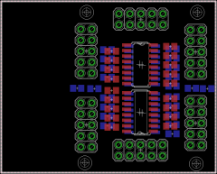
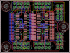
I started with Altitude's schem (thanks!) but changed basically all of the parts in the end. I've gone for a DIP20 MAX525 because there was plenty of space. This won't be too cheap -- the DIP20 version is about $10 more than the SSOIC20, and this is just a 4-channel board keeping in line with my other projects. The dimensions are 100x58.4 mm I've cascaded the J19 connections (hopefully not too close together) and added a chip select line for RC1/2. GND and AGND are on separate planes, joined at one point. Each output has a scale control (1/4 TL074) and a second stage (1/4 TL074) to either buffer (0->10.67 V) scale (0->5.33 V) or offset (-5.00->5.67 V). This can be configured with jumpers or a second control board. The offsets are generated by LM4040 precision references. This should be better than dividing the 12 V rail which can be fairly noisy. Each output then has a divider pot for attenuation. Power is via Eurorack style 2x5 DIL or AOUT style 3 pin SIL headers. Questions/comments are welcome.
-
© 2014 latigid on
-
© 2014 latigid on
-
FYI: new TTSH will come soon (1-2 months). There was somebody on MW who was looking to buy unused kits.
-
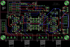
One annoying error with the AIN board: changing from LM7805 to LM4040 I've misplaced the regulator (should come after the series resistor). I don't think it's fatal as there are a few spare headers for Vref. New things: here is a simulation for a 0-10/0-5/-5-+5 V offset circuit for a MAX525 based AOUT. The aim is to build a circuit following Altitude's but probably through hole for the most part.
-
Ich kenn nichts so gut Deutsch, aber: Ich sehe ein paar Fehler: Vias auf Pads IDC Steckverbinder werden groessen als dem Headers sein. Unrouted Anschluss Man kann die "SSIP" Widerstandnetwerks bestellen, http://www.digikey.com/product-detail/en/EXB-H6E221J/R5221CT-ND/115784 http://www.ebay.com/itm/QTY-50-EXBH8E682J-PANASONIC-8-SSIP-SMD-BUSSED-RESISTOR-NETWORKS-6-8K-Ohm-/111481425911 Fuer die kleines Platten, warum nichts ein DINX2 machen? Dann man kann die 74HC165 in einer Linie montieren.
-
So, as the STM32F4 ADC reference is 3.0 V, the first amp stage must be decreased. I think it's safe to keep the supply rails at 3.3 V, as the STM32 pins can take up to 3.6 V. Anything above 3 V on the output will clip the top of the waveform though. A 59k feedback resistor in the first inverting stage will turn 5 V into 2.95. With 59k in the first stage, a cap value of 1 pF will result in a first order filter with a corner frequency of 2.7 MHz, 10 pF would give 270 kHz, 100 pF 27 kHz etc. Fc = 1/2*pi*C*Rf. So I'd recommend a 10 pF cap here. A filter on the second stage is probably not needed but I'll leave the pads in. Other recent additions (I won't bother with a picture): 12 and 3.3V travel through the same interconnect cable as the AINs. 5 V was replaced by an LM4040 precision reference The 4427 driver can be powered by any voltage (over 7 V I think) via the 12V rail or an external source anywhere up to 18 V. The trigger thresholds are less than 0.8-1.0 V for off and greater than 1.5-2.4 V for on, which are easy to get from our DOUT module. The supply voltage then sets the gate level. Switches are more centred between the jack sockets with the 2x8 DIL header at 90°. One central mounting hole was added so the boards can be stacked one on top of the other. This could be better for small breakout boxes rather than full 19" panels.
-
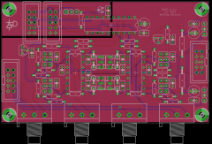
The spacing is a bit tight with 700 mil between the pots. I've enlarged the board to 100 mm and spaced the pots 900 mil/22.9 mm apart. With a bit of suggestion from Altitude I think it will be better to use an LM4040 reference in place of the linear Vreg. I will also include 4427 chips on the control board to optionally select 12 V for two (or maybe all four) gates... Edit: because I will use the same board as an output module for AOUT (+atten.), CV range switch, and gates with LEDs
